
Page 351 - Renewable Energy Devices and System with Simulations in MATLAB and ANSYS
P. 351
338 Renewable Energy Devices and Systems with Simulations in MATLAB and ANSYS ®
®
Power flow
L 2
+ C 1 DC/AC DC/AC C 2 +
V in – converter converter – V out
(a) HF Xfmr
Power flow
+ C DC/AC DC/AC C +
V in – 1 converter converter 2 – V out
(b) HF Xfmr
Power flow
L 1 L 2
+ C DC/AC DC/AC C 2 +
V in – 1 converter converter – V out
(c) HF Xfmr
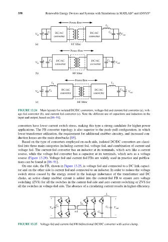
FIGURE 13.24 Main layouts for isolated DC/DC converters, voltage-fed and current-fed converter (a), volt-
age-fed converter (b), and current-fed converter (c). Note the different use of capacitors and inductors in the
input and output, based on [86–91].
converters have lower current switch stress, making this type a strong candidate for higher power
applications. The FB converter topology is also superior to the push–pull configuration, in which
lower transformer utilization, the requirement for additional snubber circuitry, and increased con-
duction losses are the main drawbacks [85].
Based on the type of converters employed on each side, isolated DC/DC converters are classi-
fied into three main categories including current fed, voltage fed, and combination of current and
voltage fed. The current-fed converter has an inductor at its terminals, which acts like a current
source, while the voltage-fed converter has a capacitor at its terminals, which acts as a voltage
source (Figure 13.24). Voltage-fed and current-fed FBs are widely used in practice and publica-
tions can be found in [86–91].
On one side, the FB, shown in Figure 13.25, is voltage fed and connected to a DC link capaci-
tor and on the other side is current fed and connected to an inductor. In order to reduce the voltage
switch stress caused by the energy stored in the leakage inductance of the transformer and DC
choke, an active clamp snubber circuit is added into the current-fed FB to ensure zero voltage
switching (ZVS) for all the switches in the current-fed side and zero current switching or ZVS for
all the switches in voltage-fed side. The absence of a circulating current results in higher efficiency.
L
+ +
L k
C
V in 1 C 2 V out
n:1 C 3
– –
FIGURE 13.25 Voltage-fed and current-fed FB bidirectional DC/DC converter with active clamp.