
Page 449 - Robot Builder's Bonanza
P. 449
418 MAKING CIRCUIT BOARDS
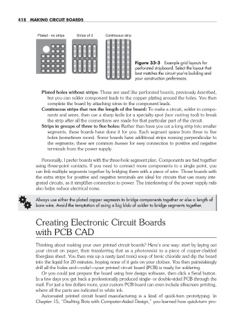
Plated - no strips Strips of 3 Continuous strip
Figure 33- 3 Example grid layouts for
perforated stripboard. Select the layout that
best matches the circuit you’re building and
your construction preferences.
Plated holes without strips: These are used like perforated boards, previously described,
but you can solder component leads to the copper plating around the holes. You then
complete the board by attaching wires to the component leads.
Continuous strips that run the length of the board: To make a circuit, solder in compo-
nents and wires, then use a sharp knife (or a specialty spot face cutting tool) to break
the strip after all the connections are made for that particular part of the circuit.
Strips in groups of three to five holes: Rather than have you cut a long strip into smaller
segments, these boards have done it for you. Each segment spans from three to five
holes (sometimes more). Some boards have additional strips running perpendicular to
the segments; these are common busses for easy connection to positive and negative
terminals from the power supply.
Personally, I prefer boards with the three- hole segment plan. Components are tied together
using three- point contacts. If you need to connect more components to a single point, you
can link multiple segments together by bridging them with a piece of wire. Those boards with
the extra strips for positive and negative terminals are ideal for circuits that use many inte-
grated circuits, as it simplifies connection to power. The interleaving of the power supply rails
also helps reduce electrical noise.
G Always use either the plated copper segments to bridge components together or else a length of
bare wire. Avoid the temptation of using a big blob of solder to bridge segments together.
Creating Electronic Circuit Boards
with PCB CAD
Thinking about making your own printed circuit boards? Here’s one way: start by laying out
your circuit on paper, then transferring that as a photoresist to a piece of copper- cladded
fiberglass sheet. You then mix up a nasty (and toxic) soup of ferric chloride and dip the board
into the liquid for 20 minutes, hoping none of it gets on your clothes. You then painstakingly
drill all the holes and— voila!—your printed circuit board (PCB) is ready for soldering.
Or you could just prepare the board using free design software, then click a Send button.
In a few days you get back a professionally produced single- or double- sided PCB through the
mail. For just a few dollars more, your custom PCB board can even include silkscreen printing,
where all the parts are indicated in white ink.
Automated printed circuit board manufacturing is a kind of quick- turn prototyping. In
Chapter 15, “Drafting Bots with Computer- Aided Design,” you learned how quick- turn pro-
33-chapter-33.indd 418 4/21/11 11:56 AM