
Page 133 - Science at the nanoscale
P. 133
RPS: PSP0007 - Science-at-Nanoscale
8:11
June 9, 2009
6.2. Electron Transport Properties in Low Dimensional Systems
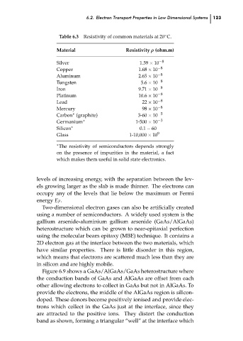
Table 6.3 Resistivity of common materials at 20 C.
◦
Material
Resistivity ρ (ohm.m)
−8
1.59 × 10
Silver
−8
Copper
1.68 × 10
−8
Aluminum
2.65 × 10
−8
5.6 × 10
Tungsten
−8
Iron
9.71 × 10
−8
Platinum
10.6 × 10
−8
22 × 10
Lead
−8
Mercury
98 × 10
−5
3-60 × 10
∗
Carbon (graphite)
−3
∗
Germanium
1-500 × 10
∗
0.1 − 60
Silicon
9
1-10,000 × 10
Glass
∗
The resistivity of semiconductors depends strongly
on the presence of impurities in the material, a fact
which makes them useful in solid state electronics.
levels of increasing energy, with the separation between the lev-
els growing larger as the slab is made thinner. The electrons can
occupy any of the levels that lie below the maximum or Fermi
energy E F .
Two-dimensional electron gases can also be artificially created
using a number of semiconductors. A widely used system is the
gallium arsenide-aluminium gallium arsenide (GaAs/AlGaAs)
heterostructure which can be grown to near-epitaxial perfection
using the molecular beam epitaxy (MBE) technique. It contains a
2D electron gas at the interface between the two materials, which 123 ch06
have similar properties. There is little disorder in this region,
which means that electrons are scattered much less than they are
in silicon and are highly mobile.
Figure 6.9 shows a GaAs/AlGaAs/GaAs heterostructure where
the conduction bands of GaAs and AlGaAs are offset from each
other allowing electrons to collect in GaAs but not in AlGaAs. To
provide the electrons, the middle of the AlGaAs region is silicon-
doped. These donors become positively ionised and provide elec-
trons which collect in the GaAs just at the interface, since they
are attracted to the positive ions. They distort the conduction
band as shown, forming a triangular “well” at the interface which