
Page 134 - Science at the nanoscale
P. 134
8:11
RPS: PSP0007 - Science-at-Nanoscale
June 9, 2009
Low-Dimensional Nanostructures
124
V
Surface
GaAs
+
+
+
AlGaAs
+
GaAs
E
Substrate
f
E c
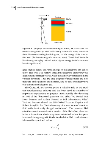
Figure 6.9.
(Right) Cross-section through a GaAs/AlGaAs/GaAs het-
erostructure grown by MBE with nearly atomically sharp interfaces.
(Left) The corresponding band diagram, i.e. the energy of the conduc-
tion band (the lowest energy electrons can have). The dashed line is the
Fermi energy (roughly defined as the highest energy that electrons can
have in equilibrium).
goes slightly below the Fermi energy so that electrons can collect
there. This well is so narrow that all the electrons there behave as
quantum-mechanical waves, with the same wave function in the
vertical direction. Thus the only degrees of freedom for the elec-
trons are in the plane of the interface, and so they are effectively a
two-dimensional electron gas.
The GaAs/AlGaAs system plays a valuable role in the mod-
ern optoelectronics industry and has been used in a number of
important experiments in physics, most notably the discovery
in 1982 of the “fractional quantum Hall effect” by Daniel Tsui,
Horst Stormer and Arthur Gossard at Bell Laboratories, USA. 1 ch06
Tsui and Stormer shared the 1998 Nobel Prize for Physics with
Robert Laughlin for “their discovery of a new form of quantum
fluid with fractionally charged excitations”. The quantum Hall
effect is a quantum-mechanical version of the Hall effect, observed
in two-dimensional electron systems subjected to low tempera-
tures and strong magnetic fields, in which the Hall conductance σ
takes on the quantised values:
e 2
σ = ν (6.18)
h
1 D. C. Tsui, H. L. Stormer and A. C. Gossard, Phys. Rev. Lett. 48, 1559 (1982).