Page 140 - Science at the nanoscale
P. 140
8:11
                                                     RPS: PSP0007 - Science-at-Nanoscale
                   June 9, 2009
                              Low-Dimensional Nanostructures
                         130
                                   of the barriers. To see this, consider the typical time to charge
                                   or discharge the island ∆t = R t C. The Heisenberg uncertainty
                                                    2
                                   relation: ∆E∆t = (e /C)R t C > h implies that R t should be much
                                                                       2
                                                                         = 25.813kW in order
                                   larger than the resistance quantum h/e
                                   for the energy uncertainty to be much smaller than the charging
                                   energy.
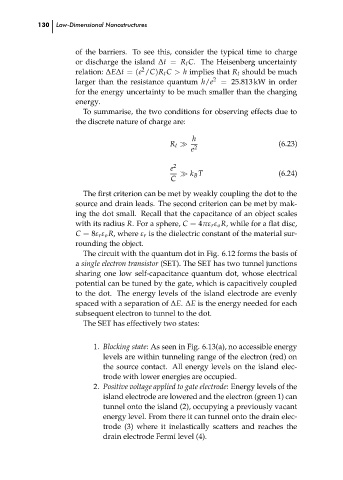
                                     To summarise, the two conditions for observing effects due to
                                   the discrete nature of charge are:
                                                                 h
                                                                                        (6.23)
                                                            R t ≫
                                                                  2
                                                                 e
                                                            2
                                                            e
                                                              ≫ k B T
                                                                                        (6.24)
                                                            C
                                     The first criterion can be met by weakly coupling the dot to the
                                   source and drain leads. The second criterion can be met by mak-
                                   ing the dot small. Recall that the capacitance of an object scales
                                   with its radius R. For a sphere, C = 4πε r ε o R, while for a flat disc,
                                   C = 8ε r ε o R, where ε r is the dielectric constant of the material sur-
                                   rounding the object.
                                     The circuit with the quantum dot in Fig. 6.12 forms the basis of
                                   a single electron transistor (SET). The SET has two tunnel junctions
                                   sharing one low self-capacitance quantum dot, whose electrical
                                   potential can be tuned by the gate, which is capacitively coupled
                                   to the dot. The energy levels of the island electrode are evenly
                                   spaced with a separation of ∆E. ∆E is the energy needed for each
                                   subsequent electron to tunnel to the dot.
                                     The SET has effectively two states:
                                        1. Blocking state: As seen in Fig. 6.13(a), no accessible energy  ch06
                                          levels are within tunneling range of the electron (red) on
                                          the source contact. All energy levels on the island elec-
                                          trode with lower energies are occupied.
                                        2. Positive voltage applied to gate electrode: Energy levels of the
                                          island electrode are lowered and the electron (green 1) can
                                          tunnel onto the island (2), occupying a previously vacant
                                          energy level. From there it can tunnel onto the drain elec-
                                          trode (3) where it inelastically scatters and reaches the
                                          drain electrode Fermi level (4).

