Page 271 - Semiconductor For Micro- and Nanotechnology An Introduction For Engineers
P. 271
Interacting Subsystems
                                                            and  ψ
                             electrons had two possible states  ψ
                                                                   where they may be found
                                                          1
                                                                2
                             in, e.g., the valence or conduction band edge. As we know from electro-
                             statics and from the polar optical phonon interaction, the energy is given
                             by the product of the incident electric field E   and the dipole moment p
                             of the electronic system. In classical terms the dipole moment is given as
                             charge times distance  p =  er  . Assume that the electric field varies little
                             in space with respect to the extension of the electronic states. Since the
                             charge of the electron has a density distribution according to the wave-
                             function  Ψ r t,(  )  , which for the unperturbed problem is a superposition
                                ,
                               (
                             Ψ r t) =   j ∑  c t()exp  – (  iω t)ψ r()  . The matrix elements read
                                          j
                                                    j
                                                        j
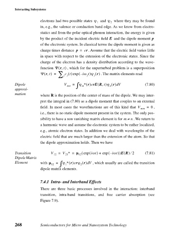
                Dipole                   V   =  ∫ ψ ∗ r()erE R t,(  )ψ r() Vd     (7.80)
                                          mn      m             n
                approxi-
                mation
                             where R is the position of the center of mass of the dipole. We may inter-
                             pret the integral in (7.80) as a dipole moment that couples to an external
                             field. In most cases the wavefunctions are of this kind that  V  mm  =  , 0
                             i.e., there is no static dipole moment present in the system. The only pos-
                             sibility to have a non vanishing matrix element is for m ≠  n  . We return to
                             a harmonic wave and assume the electronic system to be rather localized,
                             e.g., atomic electron states. In addition we deal with wavelengths of the
                             electric field that are much larger than the extension of the atom. So that
                             the dipole approximation holds. Then we have

                                                                           ⁄
                Transition        V  12  =  V ∗ =  µµ µ µ ( exp ( iωt) +  exp (  i – ωt))ER() 2  (7.81)
                                                12
                                         21
                Dipole Matrix
                Element      with µµ µµ  =  ∫ ψ ∗ r()erψ r() V  , which usually are called the transition
                                                     d
                                  12     1       2
                             dipole matrix elements.
                             7.4.1 Intra- and Interband Effects

                             There are three basic processes involved in the interaction: interband
                             transition, intra-band transitions, and free carrier absorption (see
                             Figure 7.9).


                268          Semiconductors for Micro and Nanosystem Technology

