
Page 266 - Semiconductor For Micro- and Nanotechnology An Introduction For Engineers
P. 266
Electron-Phonon
sure thermal quantities in the conductor. As we shall see, the addition of a
magnetic field produces an ever richer structure of possibilities.
Integrated The integrated thermopile exploits the thermoelectric power of different
Thermopiles: materials to produce a sophisticated temperature sensor. It also relies on
The Seebeck
massive parallelism and careful accounting of heat losses. One particu-
Effect
larly successful design [7.4] employs many alternating n-doped and p-
doped connected polysilicon wires patterned on top of a chip surface, see
Figure 7.8. The inter-metal contacts are alternately at T and T . If
hot cold
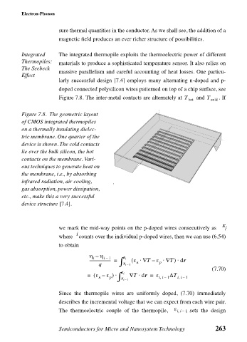
Figure 7.8. The geometric layout
of CMOS integrated thermopiles
on a thermally insulating dielec-
tric membrane. One quarter of the
device is shown. The cold contacts
lie over the bulk silicon, the hot
contacts on the membrane. Vari-
ous techniques to generate heat on
the membrane, i.e., by absorbing
infrared radiation, air cooling,
4
gas absorption, power dissipation,
etc., make this a very successful
device structure [7.4].
x
we mark the mid-way points on the p-doped wires consecutively as , i
i
where counts over the individual p-doped wires, then we can use (6.54)
to obtain
η – η i 1 x i
i
–
⋅
---------------------- = x i 1– ∫ ( ε ⋅ ∇ T – ε ⋅ ∇ T) dr
p
n
q
(7.70)
⋅
= ( ε – ε ) ⋅ x i 1– ∫ x i ∇ T dr = ε ii 1 ∆T ii 1
,
,
–
–
n
p
Since the thermopile wires are uniformly doped, (7.70) immediately
describes the incremental voltage that we can expect from each wire pair.
The thermoelectric couple of the thermopile, ε ii 1 , sets the design
,
–
Semiconductors for Micro and Nanosystem Technology 263