
Page 264 - Semiconductor For Micro- and Nanotechnology An Introduction For Engineers
P. 264
Electron-Phonon
1
µ ∝
ij
m ∗ )
( ----------------- a (7.68)
ij
a
where the exponent depends on the scattering mechanisms that are
considered. The point here is that if the band’s curvature changes, as is
illustrated in Figure 7.6, then so does the effective mass due to the
a) k z b) k z c) k z
k k k
y y y
k x k x k x
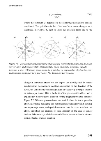
Figure 7.6. The conduction band minima of silicon are ellipsoidal in shape and lie along
the “k” axes. a) Reference state. b) Hydrostatic stress causes the minima to equally
decrease in size. c) Uniaxial stress along the x-axis has no appreciable effect on the con-
duction band minima of the y and z axes. The figures are not to scale.
change in curvature. Hence we also expect the mobility and the carrier
conductivities to change. In addition, depending on the direction of the
stress, the conductivity can change from an effectively isotropic value to
an anisotropic tensor. This is the basis of the piezoresistive effect, and is
exploited in piezoresistors, as shown for the integrated pressure sensor of
Figure 7.7. Whereas piezoresistors are useful, there is also a parasitic
effect. Electronic packaging can cause resistance changes within the chip
due to package stress, and special measures must be taken to reduce this
effect, including the addition of extra circuitry in the case of sensor
devices. When the crystal deformation is linear, we can write the piezore-
sistive effect as a tensor equation
Semiconductors for Micro and Nanosystem Technology 261