Page 260 - Semiconductor For Micro- and Nanotechnology An Introduction For Engineers
P. 260
Electron-Phonon
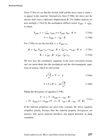
                             From (7.58a) we see that the electric field and the stress cause a strain ε
                             to appear in the material. Alternatively, from (7.58b), the stress and the
                             electric field cause a dielectric displacement  D  . For further analysis we
                                                                                   – 1
                             now multiply (7.58a) by the mechanical stiffness tensor  E  =  s
                                                                            EHT    EHT
                             to obtain
                                               – 1
                                     E    :ε =  s  :s  :σ +  E  :d  ⋅  E   or    (7.59a)
                                      EHT      EHT  EHT      EHT  HT
                                                         –
                                              σ =  E   :ε e   ⋅  E               (7.59b)
                                                   EHT     HT
                             For (7.58b) we use the fact that σ =  E  :ε
                                                            EHT  m
                                D =  d  :E   :ε +  κ   ⋅  E =  e T  :ε +  κ  ⋅  E   or  (7.59c)
                                      HT  EHT  m   σHT       HT  m    σHT
                                          E =  κ – 1  ⋅  D κ – 1  e ⋅  T  :ε     (7.59d)
                                                      –
                                                σHT      σHT   HT  m
                             We now have the constitutive equations in the most convenient format,
                             and can insert them into the mechanical and the electromagnetic equa-
                             tions of motion, which we first restate
                                                  2
                                                 ∂ u
                                                         ⋅
                                               ρ-------- =  ∇σ –  f              (7.60a)
                                                   2
                                                 ∂t
                                                              2
                                                             ∂ E
                                             ∇ ×  ∇ ×  E =  – µκ---------        (7.60b)
                                                             ∂t 2
                             Taking the divergence of equation (7.59b)

                                            ⋅
                                          ∇σ =    ∇ (⋅  E  :ε e  ⋅  E)
                                                            –
                                                       EHT    HT
                                                                                  (7.61)
                                                  (
                                                            ⋅
                                                                             ⋅
                                                                  ⋅
                                                     ⋅
                                   ⋅
                              =  ( ∇ E   ):ε +  E  : ∇ε) ( ∇ e  ) E e      ( ⋅  ∇ E)
                                                                    –
                                                        –
                                     EHT      EHT             HT       HT
                             If the material properties are piece-wise constant, the above equation
                             simplifies greatly, because then the material property divergences are
                             nonzero only across material interfaces and appear therefore as jump
                             conditions.
                             Semiconductors for Micro and Nanosystem Technology    257

