
Page 265 - Semiconductor For Micro- and Nanotechnology An Introduction For Engineers
P. 265
Interacting Subsystems
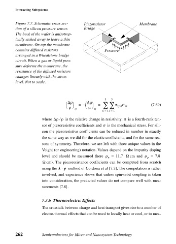
Figure 7.7. Schematic cross sec-
Bridge
tion of a silicon pressure sensor. Piezoresistor Membrane
The back of the wafer is anisotrop-
ically etched away to leave a thin
membrane. On top the membrane
contains diffused resistors Pressure
arranged in a Wheatstone bridge
circuit. When a gas or liquid pres-
sure deforms the membrane, the
resistance of the diffused resistors
changes linearly with the stress
level. Not to scale.
3 3
∆ρ ∆µ π σ
µ
------- = – ------- = ∑ ∑ ijkl kl (7.69)
ρ
ij ij
k = 1 l = 1
where ∆ρ ρ⁄ is the relative change in resistivity, is a fourth-rank ten-
π
σ
sor of piezoresistive coefficients and is the mechanical stress. For sili-
con the piezoresistive coefficients can be reduced in number in exactly
the same way as we did for the elastic coefficients, and for the same rea-
sons of symmetry. Therefore, we are left with three unique values in the
Voight (or engineering) notation. Values depend on the impurity doping
level and should be measured (here ρ = 11.7 Ω cm and ρ = 7.8
n p
Ω cm). The piezoresistance coefficients can be computed from scratch
using the kp⋅ method of Cordona et al [7.7]. The computation is rather
involved, and experience shows that unless spin-orbit coupling is taken
into consideration, the predicted values do not compare well with mea-
surements [7.8].
7.3.6 Thermoelectric Effects
The crosstalk between charge and heat transport gives rise to a number of
electro-thermal effects that can be used to locally heat or cool, or to mea-
262 Semiconductors for Micro and Nanosystem Technology