Page 262 - Semiconductor For Micro- and Nanotechnology An Introduction For Engineers
P. 262

Electron-Phonon
                                                                        and a frequency of
                             produces a strain field with a spatial period of  2d
                               ⁄
                             πcd   where   is the wave propagation velocity. At least part of this
                                        c
                             strain field is of the right shape to propagate as a Love surface acoustic
                             wave, and clever design will maximize this ratio.
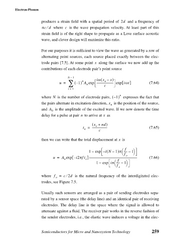
                             For our purposes it is sufficient to view the wave as generated by a row of
                             alternating point sources, each source placed exactly between the elec-
                                                       x
                             trode pairs [7.5]. At some point   along the surface we now add up the
                             contributions of each electrode pair’s point source

                                          N – 1         iω x –  x)
                                                          (
                                                            n
                                                 n
                                      u =  ∑  – (  1) A exp  ------------------------- exp [ iωt]  (7.64)
                                                   n
                                                            c
                                          i =  1
                             where N   is the number of electrode pairs,  –(  1) n   expresses the fact that
                             the pairs alternate in excitation direction, x   is the position of the source,
                                                               n
                             and  A   is the amplitude of the excited wave. If we now denote the time
                                  0
                             delay for a pulse at pair   to arrive at   as
                                                n
                                                           x
                                                      ( x +  nd)
                                                        o
                                                 t =  ----------------------      (7.65)
                                                  n
                                                         c
                                                                   x
                             then we can write that the total displacement at   is
                                                                      f
                                                                    
                                                             (
                                                    1 –  exp  – iN –  1)π ----- –  1 
                                                                      f   o  
                                  u =  A exp  – [  i2πft ]------------------------------------------------------------------------  (7.66)
                                        n
                                                  o
                                                                  f
                                                                 
                                                        1 –  exp  iπ ----- –  1 
                                                                  f   
                                                                   o
                                         ⁄
                             where  f  =  c 2d   is the natural frequency of the interdigitated elec-
                                    o
                             trodes, see Figure 7.5.
                             Usually such sensors are arranged as a pair of sending electrodes sepa-
                             rated by a sensor space (the delay line) and an identical pair of receiving
                             electrodes. The delay line is the space where the signal is allowed to
                             attenuate against a fluid. The receiver pair works in the reverse fashion of
                             the sender electrodes, i.e., the elastic wave induces a voltage in the elec-

                             Semiconductors for Micro and Nanosystem Technology    259
   257   258   259   260   261   262   263   264   265   266   267