Page 267 - Semiconductor For Micro- and Nanotechnology An Introduction For Engineers
P. 267
Interacting Subsystems
objective. For n-doped and p-doped polysilicon wires in commercial
CMOS technology we can expect to achieve a maximum of
ε = 900 µVK – 1 , with typical values lying at half that value
,
ii 1
–
[Nathan]. For design purposes, this implies that we need to ensure that
the hot and cold contacts are very well isolated from each other, which is
usually achieved by positioning the cold contacts on the bulk of the chip,
and the hot contacts on a thermally-isolated membrane. In addition, we
need many thermocouples in the thermopile, and typical designs have 50
or more pairs. Note that the large number of metal lines connecting the
thermally insulated hot and cold contacts is a misnomer, since metal is an
excellent conductor of heat. This makes the design of real thermopiles in
silicon technology very challenging, and requires the use of on-chip
amplification of the small voltages that arise when small temperature dif-
ferences have to be measured.
Seebeck Formal transport theory predicts the existence of the Seebeck effect, and
Effect in of course determines which mathematical form it should have. At the
Silicon
microscopic level, the cause of the Seebeck effect in Silicon begins with
a non-local shift in the position of the Fermi level due to the temperature
gradient [7.9]. In hotter regions, the Fermi level is shifted closer towards
the middle or intrinsic position of the bandgap than in colder regions. At
the same time, the charge carriers in the hot regions have a higher veloc-
ity than in the cold regions. In this way the hot regions deplete somewhat,
and the cold regions gain in carrier concentration. There is also a net flow
of phonons from hot to cold regions. The drag force exerted by the
phonons on the electrons further enhance the concentration of carriers
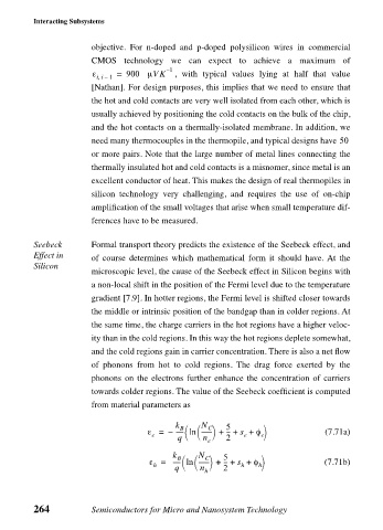
towards colder regions. The value of the Seebeck coefficient is computed
from material parameters as
k B N C 5
ε = – ----- ln ------- + --- + s + φ e (7.71a)
n
q
e
e
e 2
k B N C 5
ε = ----- ln ------- + --- + s + φ h (7.71b)
n
q
h
h
h 2
264 Semiconductors for Micro and Nanosystem Technology

