Page 284 - Semiconductor For Micro- and Nanotechnology An Introduction For Engineers
P. 284
Inhomogeneities
N
2
∑
i ∑
I
(
(
------
j'
j
i'
0
i
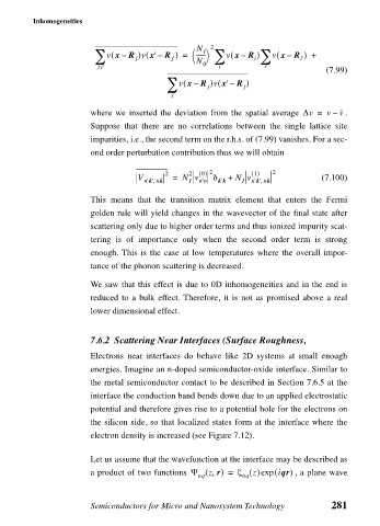
jj' v x –( R )v x' –( R ) = N ∑ v x – R ) i' v x – R ) +
(7.99)
∑ v x –( R )v x' –( R )
j
j
j
where we inserted the deviation from the spatial average ∆v = v – . v
Suppose that there are no correlations between the single lattice site
impurities, i.e., the second term on the r.h.s. of (7.99) vanishes. For a sec-
ond order perturbation contribution thus we will obtain
2 2 0 () 2 1 () 2
V = N v δ + N v (7.100)
,
,
n'k' nk I n'n k'k I n'k' nk
This means that the transition matrix element that enters the Fermi
golden rule will yield changes in the wavevector of the final state after
scattering only due to higher order terms and thus ionized impurity scat-
tering is of importance only when the second order term is strong
enough. This is the case at low temperatures where the overall impor-
tance of the phonon scattering is decreased.
We saw that this effect is due to 0D inhomogeneities and in the end is
reduced to a bulk effect. Therefore, it is not as promised above a real
lower dimensional effect.
7.6.2 Scattering Near Interfaces (Surface Roughness,
Electrons near interfaces do behave like 2D systems at small enough
energies. Imagine an n-doped semiconductor-oxide interface. Similar to
the metal semiconductor contact to be described in Section 7.6.5 at the
interface the conduction band bends down due to an applied electrostatic
potential and therefore gives rise to a potential hole for the electrons on
the silicon side, so that localized states form at the interface where the
electron density is increased (see Figure 7.12).
Let us assume that the wavefunction at the interface may be described as
a product of two functions Ψ ( z r) = ζ ()exp ( iqr) , a plane wave
,
z
nq nq
Semiconductors for Micro and Nanosystem Technology 281

