Page 286 - Semiconductor For Micro- and Nanotechnology An Introduction For Engineers
P. 286
Inhomogeneities
(
[
…
–
Fz()∆ r() +
–
V z +
δV =
∆ r()) Vz()] =
(7.101)
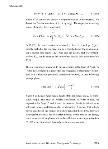
where Fz() denotes the electric field perpendicular to the interface. We
denote the Fourier transform of ∆ r() by ∆ q() . The respective scattering
matrix element is then expressed by
∞
2
∫
(
,
M kk') = e∆ q() Fz() ζ () d = e∆ q()F eff (7.102)
z
z
nq
0
In (7.102) the wavefunction is assumed to have its envelope ζ ()
z
nq
sharply peaked at the interface, which is true the higher the oxide poten-
tial is chosen (see Figure 7.12). And thus the integral that was abbrevi-
ated by F can be taken as the value of the electric field at the interface
eff
F 0() .
The only parameter unknown to this description is the form of ∆ q() . In
[7.20] the assumption is made that the roughness is statistically distrib-
uted with a Gaussian positional correlation function, i.e., the following
average given
( r') 2
r –
2
〈 ∆ r()∆ r'()〉 = ∆ exp – ------------------- (7.103)
L 2
∆
where is the root mean square height of the roughness and its corre-
L
lation length. This may be Fourier transformed in order to yield an
. and must be measured for the individual tech-
expression for ∆ q() L ∆
nological process and thus are due to fabrication. It is clear that at high
carrier densities in the channel of a MOS transistor the Si-SiO2 interface
layer quality is crucial for the carrier mobility in this zone of the device,
since an increased roughness makes the additional scattering mechanism
(7.102) very efficient and thus reduces the carrier mobility.
Semiconductors for Micro and Nanosystem Technology 283

