
Page 285 - Semiconductor For Micro- and Nanotechnology An Introduction For Engineers
P. 285
Interacting Subsystems
V =4.0V
gs
V =3.5V
3 ) 5 gs Doping 3×10 19 cm – 3
10 18 cm – V =3.0V
gs
( z
Density n() V =2.5V
gs
V =2.0V
gs
V =1.5V
gs
V =1.0V and V =0.5V
gs gs
0
0 1 2 3
6
–
(
Distance z from oxide 10 cm)
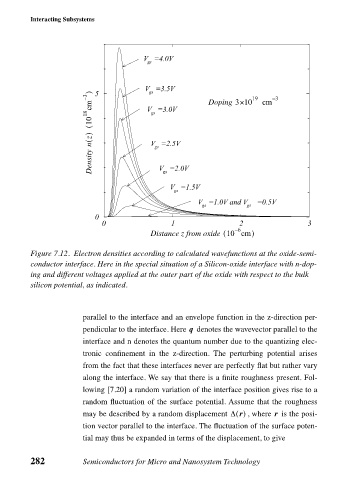
Figure 7.12. Electron densities according to calculated wavefunctions at the oxide-semi-
conductor interface. Here in the special situation of a Silicon-oxide interface with n-dop-
ing and different voltages applied at the outer part of the oxide with respect to the bulk
silicon potential, as indicated.
parallel to the interface and an envelope function in the z-direction per-
q
pendicular to the interface. Here denotes the wavevector parallel to the
interface and n denotes the quantum number due to the quantizing elec-
tronic confinement in the z-direction. The perturbing potential arises
from the fact that these interfaces never are perfectly flat but rather vary
along the interface. We say that there is a finite roughness present. Fol-
lowing [7.20] a random variation of the interface position gives rise to a
random fluctuation of the surface potential. Assume that the roughness
may be described by a random displacement ∆ r() , where is the posi-
r
tion vector parallel to the interface. The fluctuation of the surface poten-
tial may thus be expanded in terms of the displacement, to give
282 Semiconductors for Micro and Nanosystem Technology