
Page 61 - Semiconductor For Micro- and Nanotechnology An Introduction For Engineers
P. 61
The Crystal Lattice System
1
h
T
2∫
•
--- (
d
U =
–
i
i
Ω ∇ u ) • E ∇ u V (2.25)
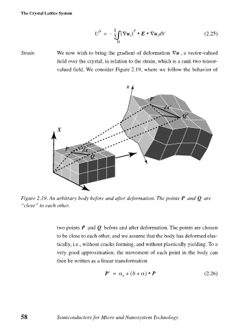
Strain We now wish to bring the gradient of deformation u∇ , a vector-valued
field over the crystal, in relation to the strain, which is a rank two tensor-
valued field. We consider Figure 2.19, where we follow the behavior of
x
P′
dx′
Q′′ ′′
X
P dx
Q
P
Figure 2.19. An arbitrary body before and after deformation. The points and Q are
“close” to each other.
P
two points and Q before and after deformation. The points are chosen
to be close to each other, and we assume that the body has deformed elas-
tically, i.e., without cracks forming, and without plastically yielding. To a
very good approximation, the movement of each point in the body can
then be written as a linear transformation
•
P′ = α + ( δ + α) P (2.26)
o
58 Semiconductors for Micro and Nanosystem Technology