Page 60 - Semiconductor For Micro- and Nanotechnology An Introduction For Engineers
P. 60
Elastic Properties: The Stressed Uniform Lattice
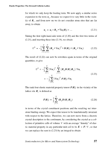
                             for which we only keep the leading term. We now apply a similar series
                             expansion to the term u  , because we expect it to vary little in the vicin-
                                                j
                             ity of  R  , and from now on we do not consider atom sites that are far
                                   i
                             away, to obtain
                                            u =  u +  R •  ∇ u R() +  …           (2.21)
                                             j    i   ij   i  i
                             Taking the first right-hand-side term of (2.20) and the first two terms of
                             (2.21), and inserting these into (2.19), we obtain
                                           N  N
                                    h    1               T
                                                              (
                                                                  •
                                  U =   – --- ∑  ∑  ( R •  ∇ u ) •  DR ) ( R •  ∇ u )  (2.22)
                                                        i
                                                                     ij
                                                   ij
                                                                           i
                                                                i
                                         4
                                          i =  1  j =  1
                             The result of (2.22) can now be rewritten again in terms of the original
                             quantities, to give
                                              N        N
                                                   i ∑
                                       h    1        T
                                                               (
                                     U =   – --- ∑ ( ∇ u ) :  { R DR )R }: u∇  i
                                                                 i
                                                                    ij
                                                            ij
                                            4
                                             i =  1   j =  1
                                                                                  (2.23)
                                                  N
                                                1        T
                                            =  –  --- ∑ ( ∇ u ) :FR(): u∇  i
                                                       i
                                                              i
                                                2
                                                 i =  1
                             The rank four elastic material property tensor FR   in the vicinity of the
                                                                   ()
                                                                     i
                             lattice site R   is defined as
                                       i
                                                     N
                                                   1
                                           FR() =  --- ∑  ( R DR(  )R )           (2.24)
                                               i          ij   i  ij
                                                   2
                                                    j =  1
                             in terms of the crystal constituent positions and the resulting net inter-
                             atom binding energy. We expect this tensor to be translationally invariant
                             with respect to the lattice. Therefore, we can now move from a discrete
                             crystal description to the continuum, by considering the crystal as a col-
                                                          V
                             lection of primitive cells of volume   with an average “density” of elas-
                                                                              ⁄
                             tic material property in any particular unit cell to be  E =  F V  , so that
                             we can replace the sum in (2.23) by an integral to obtain
                             Semiconductors for Micro and Nanosystem Technology      57

