Page 56 - Semiconductor For Micro- and Nanotechnology An Introduction For Engineers
P. 56
Elastic Properties: The Stressed Uniform Lattice
– [
D 1 –(
(
β r –
E r() =
exp
eq
e
and the equilibrium bond
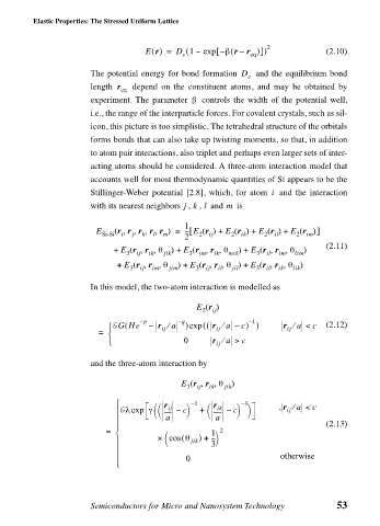
The potential energy for bond formation D r )]) 2 (2.10)
e
length r depend on the constituent atoms, and may be obtained by
eq
β
experiment. The parameter controls the width of the potential well,
i.e., the range of the interparticle forces. For covalent crystals, such as sil-
icon, this picture is too simplistic. The tetrahedral structure of the orbitals
forms bonds that can also take up twisting moments, so that, in addition
to atom pair interactions, also triplet and perhaps even larger sets of inter-
acting atoms should be considered. A three-atom interaction model that
accounts well for most thermodynamic quantities of Si appears to be the
i
Stillinger-Weber potential [2.8], which, for atom and the interaction
with its nearest neighbors , , and m is
j kl
1
,,
,
,
E Si-Si ( r r r r r ) = --- E r() +[ 2 ij E r ) + E r() + E r )]
(
(
m
il
2
im
2
ik
2
l
i
j
k
2
(
+ E r ,( r , θ ) + E r , r , θ ) + E r , r , θ ) (2.11)
(
3 ij ik jik 3 im ik mik 3 il im lim
,
(
(
+ E r ,( r , θ ) + E r , r θ ) + E r , r , θ )
3 ij im jim 3 ij il jil 3 il ik lik
In this model, the two-atom interaction is modelled as
E r()
2 ij
–
1
EGHe – p – r ⁄ a – q )exp ( ( r ⁄ a – c) ) r ⁄ a < c (2.12)
(
= ij ij ij
0 r ⁄ a > c
ij
and the three-atom interaction by
E r , r , θ )
(
ij
ik
jik
3
r – 1 r – 1
Eλexp γ ----- – c + ------ – c , r ⁄ a < c
ik
ij
ij
a a
(2.13)
= 1 2
× cos θ ( jik ) + ---
3
otherwise
0
Semiconductors for Micro and Nanosystem Technology 53

