
Page 209 - Semiconductor Manufacturing Handbook
P. 209
Geng(SMH)_CH14.qxd 04/04/2005 19:52 Page 14.10
CHEMICAL VAPOR DEPOSITION
14.10 WAFER PROCESSING
14.2.6 Wafer Temperature
Rarely is it practical to measure the wafer temperature directly. However a uniform, well-controlled
temperature is often essential for achieving a uniform, high-quality deposition. The two most com-
mon ways of achieving temperature uniformity are to maintain the entire chamber at a single tem-
perature (hot-wall reactor) or to place the wafer on a large thermal mass. As will be mentioned
later, hot-wall reactors deposit on all surfaces, hurting gas utilization and increasing particle risk.
Thus they are not as commonly used these days. However, they are hard to beat for achieving
excellent wafer temperature uniformity. In cold-wall reactors, the wafer is placed on a heated plat-
en and absorbs thermal energy both from conductive and radiative heat transfer. It also loses heat
to its surroundings by the same mechanisms. As a result its equilibrium temperature will be less
than the platen temperature. How much less depends on a number of factors—wafer platen gap,
gas type and pressure, and wafer emissivity. An excellent description of these effects is provided
by Hasper et. al. 13
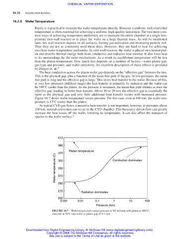
The heat conduction across the platen wafer gap depends on the “effective gap” between the two.
This is the physical gap, plus a function of the mean free path of the gas. At low pressures, the mean
free path is long and the effective gap is large. This slows heat transfer to the wafer. Because of this,
at very low pressures (millitorr range) the heat transfer is primarily by radiation and the wafer can
be 100°C cooler than the platen. As the pressure is increased, the mean free path shrinks as does the
effective gap, leading to better heat transfer. Above 10 or 20 torr, the effective gap is essentially the
same as the physical gap and very little additional heat transfer occurs with increased pressure.
Figure 14.7 shows wafer temperature versus pressure. For this case, even at 100 torr, the wafer tem-
perature is 13°C cooler than the platen.
At typical CVD gas flows, convective heat transfer is not important, however, at pressures above
100 torr, natural convection can occur in the CVD chamber. This buoyancy-driven flow can greatly
increase the heat losses off the wafer, lowering its temperature. It can also affect the transport of
species to the wafer surface. 4
410
390
Platen temperature
370 Conduction dominates
Wafer temperature (C) 350
330
310
290
270 Radiation dominates
250
0.001 0.01 0.1 1 10 100
Pressure (torr)
FIGURE 14.7 Wafer temperature versus pressure in N2 ambient with platen at 400°C,
chamber at 50°C and wafer to platen gap of 0.1 mm.
Downloaded from Digital Engineering Library @ McGraw-Hill (www.digitalengineeringlibrary.com)
Copyright © 2004 The McGraw-Hill Companies. All rights reserved.
Any use is subject to the Terms of Use as given at the website.