
Page 206 - Semiconductor Manufacturing Handbook
P. 206
Geng(SMH)_CH14.qxd 04/04/2005 19:52 Page 14.7
CHEMICAL VAPOR DEPOSITION
CHEMICAL VAPOR DEPOSITION 14.7
Inductive
coils
RF in
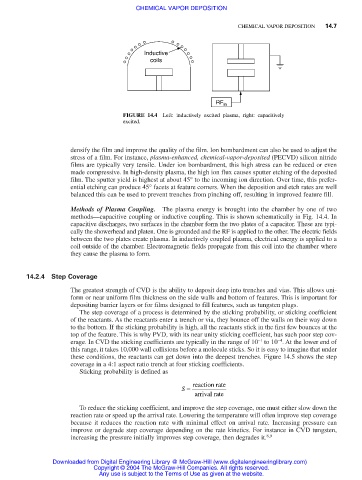
FIGURE 14.4 Left: inductively excited plasma, right: capacitively
excited.
densify the film and improve the quality of the film. Ion bombardment can also be used to adjust the
stress of a film. For instance, plasma-enhanced, chemical-vapor-deposited (PECVD) silicon nitride
films are typically very tensile. Under ion bombardment, this high stress can be reduced or even
made compressive. In high-density plasma, the high ion flux causes sputter etching of the deposited
film. The sputter yield is highest at about 45° to the incoming ion direction. Over time, this prefer-
ential etching can produce 45° facets at feature corners. When the deposition and etch rates are well
balanced this can be used to prevent trenches from pinching off, resulting in improved feature fill.
Methods of Plasma Coupling. The plasma energy is brought into the chamber by one of two
methods—capacitive coupling or inductive coupling. This is shown schematically in Fig. 14.4. In
capacitive discharges, two surfaces in the chamber form the two plates of a capacitor. These are typi-
cally the showerhead and platen. One is grounded and the RF is applied to the other. The electric fields
between the two plates create plasma. In inductively coupled plasma, electrical energy is applied to a
coil outside of the chamber. Electromagnetic fields propagate from this coil into the chamber where
they cause the plasma to form.
14.2.4 Step Coverage
The greatest strength of CVD is the ability to deposit deep into trenches and vias. This allows uni-
form or near uniform film thickness on the side walls and bottom of features. This is important for
depositing barrier layers or for films designed to fill features, such as tungsten plugs.
The step coverage of a process is determined by the sticking probability, or sticking coefficient
of the reactants. As the reactants enter a trench or via, they bounce off the walls on their way down
to the bottom. If the sticking probability is high, all the reactants stick in the first few bounces at the
top of the feature. This is why PVD, with its near unity sticking coefficient, has such poor step cov-
−1
−4
erage. In CVD the sticking coefficients are typically in the range of 10 to 10 . At the lower end of
this range, it takes 10,000 wall collisions before a molecule sticks. So it is easy to imagine that under
these conditions, the reactants can get down into the deepest trenches. Figure 14.5 shows the step
coverage in a 4:1 aspect ratio trench at four sticking coefficients.
Sticking probability is defined as
S = reaction rate
arrival rate
To reduce the sticking coefficient, and improve the step coverage, one must either slow down the
reaction rate or speed up the arrival rate. Lowering the temperature will often improve step coverage
because it reduces the reaction rate with minimal effect on arrival rate. Increasing pressure can
improve or degrade step coverage depending on the rate kinetics. For instance in CVD tungsten,
increasing the pressure initially improves step coverage, then degrades it. 8,9
Downloaded from Digital Engineering Library @ McGraw-Hill (www.digitalengineeringlibrary.com)
Copyright © 2004 The McGraw-Hill Companies. All rights reserved.
Any use is subject to the Terms of Use as given at the website.