
Page 202 - Semiconductor Manufacturing Handbook
P. 202
Geng(SMH)_CH14.qxd 04/04/2005 19:52 Page 14.3
CHEMICAL VAPOR DEPOSITION
CHEMICAL VAPOR DEPOSITION 14.3
formed, layers of metal lines separated by dielectric are laid down, forming the interconnect struc-
ture. When aluminum is used as the primary conductor, CVD tungsten provides the conductive medi-
um between metal layers. CVD is also used for the dielectric separating metal layers. This could be
CVD SiO , fluorinated SiO , or carbon-doped SiO (the latter two low-k films being used to reduce
2 2 2
the capacitance of the circuit). For copper metalization, the diffusion barrier between copper and
oxide may be deposited by CVD. Once complete, the wafer is given a scratch protection or passiva-
tion layer, typically silicon nitride or oxynitride, deposited by plasma-enhanced CVD.
14.2 THEORY
The theoretical study of CVD focuses on two areas—the transport of gases to and from the wafer,
and the chemical reactions that take place both on the wafer and in transit.
14.2.1 Mass Transfer
In order to deposit a CVD film, the reactants must be transported from the inlet to the wafer surface.
For many processes, the deposition rate is limited by how fast this takes place. Additionally, film uni-
formity can be strongly dependent on mass-transfer rates.
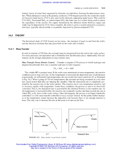
Mass Transfer Versus Kinetic Control. Consider a tungsten CVD process in which hydrogen and
tungsten hexafluoride flow into a chamber and react to form tungsten:
3H + WF → W + 6HF
2 6
The volatile HF is pumped away. If the wafer were maintained at room temperature, the reaction
would proceed at near zero rate. As the temperature is increased, the deposition rate would increase
exponentially. At sufficiently high temperature, the rate would slow down and level off, as illustrated
in Fig. 14.2. What is going on? At low temperatures, the reactants are being consumed at a very slow
rate, much slower than they are entering the chamber. Thus the deposition rate is completely gov-
erned by the reaction rate on the wafer surface. This reaction rate is very temperature sensitive, and
so increases rapidly with temperature. Under these conditions, the process is said to be kinetically
controlled. That is, the deposition rate is governed by the chemical kinetics or the reaction rate. As
the temperature is increased further, the reaction rate eventually reaches and then exceeds the rate at
which WF or H arrive at the wafer surface. Once that happens, the process is no longer kinetically
6
2
controlled; it is now mass-transfer controlled or mass-transfer limited. At this point, further increas-
es to the temperature cannot increase the deposition rate because there is not enough material to
react. The only way to increase the rate at this point is to turn up the flow.
Mass transfer
Ln (rate) Rate Kinetic
Kinetic
Mass transfer
1/T Reactant flow
FIGURE 14.2 Mass transfer versus kinetic control.
Downloaded from Digital Engineering Library @ McGraw-Hill (www.digitalengineeringlibrary.com)
Copyright © 2004 The McGraw-Hill Companies. All rights reserved.
Any use is subject to the Terms of Use as given at the website.