
Page 201 - Semiconductor Manufacturing Handbook
P. 201
Geng(SMH)_CH14.qxd 04/04/2005 19:52 Page 14.2
CHEMICAL VAPOR DEPOSITION
14.2 WAFER PROCESSING
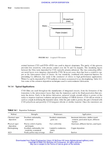
Showerhead
(inlet)
Wafer
Platen (heater)
Exhaust
FIGURE 14.1 A typical CVD reactor.
existed between CVD and PVD—PVD was used to deposit aluminum. The purity of this process
provided low resistivity with precise control over the Si and Cu dopants. The insulating layers
between the films were deposited by CVD, typically plasma enhanced. The vias connecting differ-
ent metal layers were tungsten, deposited by CVD. In recent years, there has been a switch to cop-
per as the interconnect metal of choice. Its low resistivity, combined with improved barriers for
preventing Cu diffusion, has made it the conductor of choice in high performance applications.
While Cu can be deposited by CVD methods, it is more economical to use electroplating. Table 14.1
lists some of the common deposition techniques used in semiconductor fabrication.
14.1.4 Typical Applications
CVD films are used throughout the manufacture of integrated circuits, from the formation of the
transistors to the interconnect layers that wire the transistors and in the final passivation that pro-
tects the device. Early in the device fabrication, epitaxial (single crystal) silicon is grown on the
wafer to improve transistor isolation and prevent latchup of CMOS devices. CVD silicon nitride is
used as a mask in defining the transistor areas. After the gate oxide is grown, the gate is formed with
CVD polysilicon and possibly CVD tungsten silicide or similar material. Once the transistors are
TABLE 14.1 Deposition Techniques
Method Strengths Weaknesses Applications
Chemical vapor Excellent conformality, Residual contaminants, Intermetal dielectrics, shallow trench
deposition economical grain size isolation, passivation layers, diffusion
barriers
Physical vapor Precise control of purity Poor conformity Aluminum, diffusion barriers, seed layers
deposition and dopants
Electroplating Excellent conformality, low Limited to conductors, Copper deposition
resistivity, economical purity
ALD Nearly perfect step coverage Slow Barriers
Downloaded from Digital Engineering Library @ McGraw-Hill (www.digitalengineeringlibrary.com)
Copyright © 2004 The McGraw-Hill Companies. All rights reserved.
Any use is subject to the Terms of Use as given at the website.