
Page 196 - Semiconductor Manufacturing Handbook
P. 196
Geng(SMH)_CH13.qxd 04/04/2005 19:51 Page 13.19
PHYSICAL VAPOR DEPOSITION
PHYSICAL VAPOR DEPOSITION 13.19
13.8 LAYERS DEPOSITED USING SPUTTERING
As previously mentioned, sputtering allows the deposition of almost any kind of material. It allows
the deposition of a free choice of metals, including those with high melting temperature. Depending
on the target size and material, target prices can vary a lot (e.g., Al1Si target 10 in × 5 mm: $1,000;
Pt target 10 in × 5 mm: $18,000). All alloys can be deposited using sputtering, depending on the
availability of targets for the specific sputtering system. Multilayer structures can be deposited using
multiple target sputter equipment with apertures to prevent cross contamination of targets. Chemical
compounds (dielectric materials, insulators, metal oxides) can be deposited either using specific
compound targets (mostly sintered material) and/or using reactive sputtering. A typical configuration
is using a metal or semiconductor material target and a reactive ambient gas atmosphere (O , N ) to
2 2
build oxide or nitride layers. A selection of materials and physical properties (Table 13.1) is given
below:
Metals: Au, Pt, Pd, Ni, Ti, Al, Cr, Mo
Alloys: NiCr, CrSi, TiW
Multilayers: Cr-Al, Ti-Au, Ti-Pd-Au, Ti-TiN-Au, Ti-TiWN-Au, NiCr-Ni-Au, SnO , Cr-Al
2
Chemical compounds:Al O , SnO , SiO , ZnO, Ga O , HfB , NiO, V O , Mo O , In O , glass
2 3 2 2 2 3 2 2 5 2 3 2 3
(Pyrex)
13.8.1 Step Coverage
An important issue in all coating processes is step coverage of textured and patterned substrate sur-
faces. Poor step coverage can lead to microcracks and interruption or breaking of a layer coating.
Vacuum evaporation deposition follows the cosine law with the vapor particles coming straight from
a point vapor source in high vacuum with little collisions and scattering. The subsequent coating
process is almost anisotropic, i.e., surfaces facing the vapor source are coated whereas the ones per-
pendicular to those remain almost uncoated, leading to poor step coverage. This characteristic, how-
ever, favors lithographic lift-off processes as patterning processes. Sputter deposition exhibits a large
area vapor source and higher process pressures leading to higher frequency of collisions between
vapor particles. In consequence, the vapor particles approach the substrate surface from more random
directions leading to higher deposition isotropy and better step coverage. In comparison, chemical
vapor deposition (CVD) layers almost always feature better step coverage than PVD layers. Process
pressures in CVD are typically higher than in PVD. Furthermore, the source is a strong constant gas
flow of process gases, needed as precursors for the layer (e.g., 3 sccm methylsilane in 200 sccm
hydrogen at 3.5 l/min total flow for LPCVD silicon carbide deposition). This leads to high particle
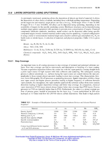
TABLE 13.1 Examples of Metallization Systems Used in Semiconductor Devices and Selected Physical
Properties 6
Material Al Au Pt Mo HfB
2
3
Density [kg/m ] 19300 2700 21500 10200 11200
Thermal conductivity l [W/mK] 237 317 71.6 138 41.8
Melting point T /°C 660 1000 1768.4 2623 3250
m
Specific heat capacity [J/KgK] 897 129 133 251 25.1
Specific resistance/µΩcm 2.4 2.2 9.6 4.85 253 ±5
Passivation layer Si N / – – Si N / Si N /
3 4 3 4 3 4
SiO SiO SiO /TaN
2 2 2
Contact layer/diffusion barrier required Ti/ Ti/ Ti
on Si and SOI substrates TiWN TiWN
Downloaded from Digital Engineering Library @ McGraw-Hill (www.digitalengineeringlibrary.com)
Copyright © 2004 The McGraw-Hill Companies. All rights reserved.
Any use is subject to the Terms of Use as given at the website.