
Page 191 - Semiconductor Manufacturing Handbook
P. 191
Geng(SMH)_CH13.qxd 04/04/2005 19:51 Page 13.14
PHYSICAL VAPOR DEPOSITION
13.14 WAFER PROCESSING
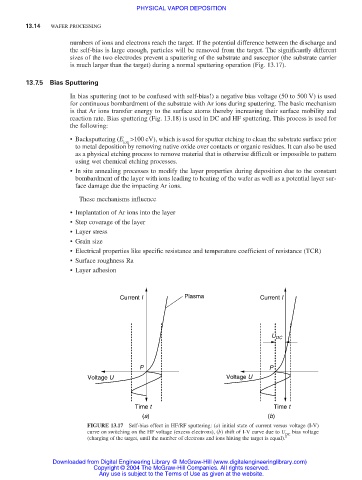
numbers of ions and electrons reach the target. If the potential difference between the discharge and
the self-bias is large enough, particles will be removed from the target. The significantly different
sizes of the two electrodes prevent a sputtering of the substrate and susceptor (the substrate carrier
is much larger than the target) during a normal sputtering operation (Fig. 13.17).
13.7.5 Bias Sputtering
In bias sputtering (not to be confused with self-bias!) a negative bias voltage (50 to 500 V) is used
for continuous bombardment of the substrate with Ar ions during sputtering. The basic mechanism
is that Ar ions transfer energy to the surface atoms thereby increasing their surface mobility and
reaction rate. Bias sputtering (Fig. 13.18) is used in DC and HF sputtering. This process is used for
the following:
• Backsputtering (E >100 eV), which is used for sputter etching to clean the substrate surface prior
ion
to metal deposition by removing native oxide over contacts or organic residues. It can also be used
as a physical etching process to remove material that is otherwise difficult or impossible to pattern
using wet chemical etching processes.
• In situ annealing processes to modify the layer properties during deposition due to the constant
bombardment of the layer with ions leading to heating of the wafer as well as a potential layer sur-
face damage due the impacting Ar ions.
These mechanisms influence
• Implantation of Ar ions into the layer
• Step coverage of the layer
• Layer stress
• Grain size
• Electrical properties like specific resistance and temperature coefficient of resistance (TCR)
• Surface roughness Ra
• Layer adhesion
Current I Plasma Current I
U DC
P P
Voltage U Voltage U
Time t Time t
(a) (b)
FIGURE 13.17 Self-bias effect in HF/RF sputtering: (a) initial state of current versus voltage (I-V)
curve on switching on the HF voltage (excess electrons), (b) shift of I-V curve due to U bias voltage
DC
(charging of the target, until the number of electrons and ions hitting the target is equal). 1
Downloaded from Digital Engineering Library @ McGraw-Hill (www.digitalengineeringlibrary.com)
Copyright © 2004 The McGraw-Hill Companies. All rights reserved.
Any use is subject to the Terms of Use as given at the website.