Page 192 - Semiconductor Manufacturing Handbook
P. 192

Geng(SMH)_CH13.qxd  04/04/2005  19:51  Page 13.15


                                                    PHYSICAL VAPOR DEPOSITION

                                                                               PHYSICAL VAPOR DEPOSITION  13.15
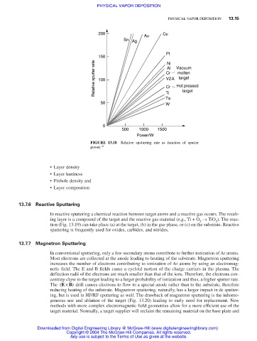

                                                    200                      Cu
                                                                      Au
                                                              Sn  Ag

                                                                              Pt
                                                    150                        Ni
                                                   Relative sputter rate  100  Cr  Vacuum
                                                                               Al
                                                                                   molten
                                                                                   target
                                                                              V2A
                                                                                  Hot pressed
                                                                              Cr
                                                                              Ti
                                                                              Ta    target
                                                     50                       W


                                                      0
                                                             500    1000   1500
                                                                   Power/W
                                                 FIGURE 13.18  Relative sputtering rate as function of sputter
                                                 power. 10


                                  • Layer density
                                  • Layer hardness
                                  • Pinhole density and
                                  • Layer composition


                      13.7.6 Reactive Sputtering

                                  In reactive sputtering a chemical reaction between target atoms and a reactive gas occurs. The result-
                                  ing layer is a compound of the target and the reactive gas material (e.g., Ti + O → TiO ). The reac-
                                                                                           2     2
                                  tion (Fig. 13.19) can take place (a) at the target, (b) in the gas-phase, or (c) on the substrate. Reactive
                                  sputtering is frequently used for oxides, carbides, and nitrides.

                      13.7.7 Magnetron Sputtering
                                  In conventional sputtering, only a few secondary atoms contribute to further ionization of Ar atoms.
                                  Most electrons are collected at the anode leading to heating of the substrate. Magnetron sputtering
                                  increases the number of electrons contributing to ionization of Ar atoms by using an electromag-
                                  netic field. The E and B fields cause a cycloid motion of the charge carriers in the plasma. The
                                  deflection radii of the electrons are much smaller than that of the ions. Therefore, the electrons con-
                                  centrate close to the target leading to a larger probability of ionization and thus, a higher sputter rate.
                                       r
                                         r
                                  The  (EB×  )  drift causes electrons to flow to a special anode rather than to the substrate, therefore
                                  reducing heating of the substrate. Magnetron sputtering, naturally, has a larger impact in dc sputter-
                                  ing, but is used in HF/RF sputtering as well. The drawback of magnetron sputtering is the inhomo-
                                  geneous use and ablation of the target (Fig. 13.20) leading to early need for replacement. New
                                  methods with more complex electromagnetic field geometries allow for a more efficient use of the
                                  target material. Normally, a target supplier will reclaim the remaining material on the base plate and


                             Downloaded from Digital Engineering Library @ McGraw-Hill (www.digitalengineeringlibrary.com)
                                        Copyright © 2004 The McGraw-Hill Companies. All rights reserved.
                                          Any use is subject to the Terms of Use as given at the website.
   187   188   189   190   191   192   193   194   195   196   197