
Page 189 - Semiconductor Manufacturing Handbook
P. 189
Geng(SMH)_CH13.qxd 04/04/2005 19:51 Page 13.12
PHYSICAL VAPOR DEPOSITION
13.12 WAFER PROCESSING
characterization are x-ray diffraction (XRD), electron dispersive x-ray spectroscopy/wavelength
dispersive x-ray spectroscopy (EDX/WDX), Auger electron spectroscopy (AES), scanning electron
microscope (SEM), and transmission electron microscope (TEM). XRD is used to determine the
crystallinity and texture of the layers. A broader peak signifies smaller grain size. EDX/WDX is used
to determine the composition of the layers, to detect contamination, stoichiometry of compound layers
and reaction of donors, and dopant materials with underlying base layers.
Zones 1–3 as in evaporation
Zone T—fiber-type closely packed layer with smooth surface
13.7 SPUTTER EQUIPMENT
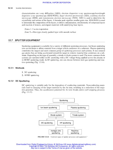
Sputtering equipment is available for a variety of different sputtering processes. Ion beam sputtering
uses an ion beam to ablate material from a target which condenses on a substrate. Plasma sputtering
constitutes the largest and most common group of sputtering processes and systems. It uses ionized
gas atoms that are being accelerated toward the target to remove material that condenses on a sub-
strate. Depending on the type of assembly, a triode or diode system is used. The more common diode
systems are operated either in DC sputtering with a DC voltage being applied across the plasma or
in HF/RF sputtering mode. In RF sputtering, one can choose between inert gas sputtering and reac-
tive sputtering (Fig. 13.14).
13.7.1 Methods
1. DC-sputtering
2. HF/RF sputtering
13.7.2 DC Sputtering
DC sputtering is suitable only for the deposition of conducting materials. Nonconducting mate-
rials lead to charging of the target material by the Ar ions, resulting in a reduction of the nega-
tive potential. Thus, the acceleration potential for Ar ions breaks down (self-stopping process).
(Fig. 13.15)
Sputtering
Ion beam sputtering Plasma sputtering
Diode system Triode system
DC-sputtering HF-sputtering
Inertgas (Ar) Reactive
sputtering sputtering
FIGURE 13.14 Common types of sputter processes and equipment. 2
Downloaded from Digital Engineering Library @ McGraw-Hill (www.digitalengineeringlibrary.com)
Copyright © 2004 The McGraw-Hill Companies. All rights reserved.
Any use is subject to the Terms of Use as given at the website.