
Page 184 - Semiconductor Manufacturing Handbook
P. 184
Geng(SMH)_CH13.qxd 04/04/2005 19:51 Page 13.7
PHYSICAL VAPOR DEPOSITION
PHYSICAL VAPOR DEPOSITION 13.7
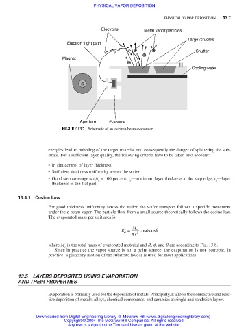
Electrons Metal vapor particles
Target/crucible
Electron flight path
+ + Shutter
+
Magnet
+
Cooling water
S
Aperture E-source
FIGURE 13.7 Schematic of an electron-beam evaporator.
energies lead to bubbling of the target material and consequently the danger of splattering the sub-
strate. For a sufficient layer quality, the following criteria have to be taken into account:
• In situ control of layer thickness
• Sufficient thickness uniformity across the wafer
• Good step coverage = t /t × 100 percent; t —minimum layer thickness at the step edge, t —layer
s n s n
thickness in the flat part
13.4.1 Cosine Law
For good thickness uniformity across the wafer, the wafer transport follows a specific movement
under the e-beam vapor. The particle flow from a small source theoretically follows the cosine law.
The evaporated mass per unit area is
R = M e cos f cos q
D 2
p r
where M is the total mass of evaporated material and R, f, and q are according to Fig. 13.8.
e
Since in practice the vapor source is not a point source, the evaporation is not isotropic. In
practice, a planetary motion of the substrate holder is used for most applications.
13.5 LAYERS DEPOSITED USING EVAPORATION
AND THEIR PROPERTIES
Evaporation is primarily used for the deposition of metals. Principally, it allows the nonreactive and reac-
tive deposition of metals, alloys, chemical compounds, and ceramics as single and sandwich layers.
Downloaded from Digital Engineering Library @ McGraw-Hill (www.digitalengineeringlibrary.com)
Copyright © 2004 The McGraw-Hill Companies. All rights reserved.
Any use is subject to the Terms of Use as given at the website.