
Page 187 - Semiconductor Manufacturing Handbook
P. 187
Geng(SMH)_CH13.qxd 04/04/2005 19:51 Page 13.10
PHYSICAL VAPOR DEPOSITION
13.10 WAFER PROCESSING
13.6.2 Mechanism
Ions are created through plasma discharge between two electrodes. Ionization occurs through inelas-
tic collisions between free electrons and gas molecules (in most cases Ar). The required ionization
energy (15.7 eV for Ar) stems from the electron kinetic energy. The kinetic energy of the Ar ions
after the acceleration by the electric field between the cathode and anode is between 10 eV and sev-
eral 1000 eV. On collision with the substrate, the Ar ions transfer a part of their kinetic energy to a
confined volume (ca. 1000 atoms) of the lattice atoms through a series of quasi-elastic collisions.
Some target atoms are diffracted toward the surface. If their energy is larger than the surface bind-
ing energy, they leave the lattice. The removed target atoms typically have 3 to 10 eV of energy. The
mean quantity of removed atoms or sputtering yield S is given by
S = number of removed target atoms
number of colliding ions
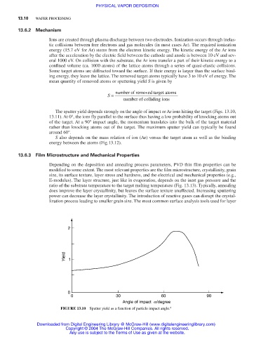
The sputter yield depends strongly on the angle of impact or Ar ions hitting the target (Figs. 13.10,
13.11). At 0°, the ions fly parallel to the surface thus having a low probability of knocking atoms out
of the target. At a 90° impact angle, the momentum translates into the bulk of the target material
rather than knocking atoms out of the target. The maximum sputter yield can typically be found
around 60°.
S also depends on the mass relation of ion (Ar) versus the target atom as well as the binding
energy between the atoms (Fig.13.12).
13.6.3 Film Microstructure and Mechanical Properties
Depending on the deposition and annealing process parameters, PVD thin film properties can be
modified to some extent. The most relevant properties are the film microstructure, crystallinity, grain
size, its surface texture, layer stress and hardness, and the electrical and mechanical properties (e.g.,
E-modulus). The layer structure, just like in evaporation, depends on the inert gas pressure and the
ratio of the substrate temperature to the target melting temperature (Fig. 13.13). Typically, annealing
does improve the layer crystallinity, but leaves the surface texture unaffected. Increasing sputtering
power can decrease the layer crystallinity. The introduction of reactive gases can disrupt the crystal-
lization process leading to smaller grain size. The most common surface analysis tools used for layer
2
Yield 1
0
0 30 60 90
Angle of impact a/degree
FIGURE 13.10 Sputter yield as a function of particle impact angle. 4
Downloaded from Digital Engineering Library @ McGraw-Hill (www.digitalengineeringlibrary.com)
Copyright © 2004 The McGraw-Hill Companies. All rights reserved.
Any use is subject to the Terms of Use as given at the website.