
Page 183 - Semiconductor Manufacturing Handbook
P. 183
Geng(SMH)_CH13.qxd 04/04/2005 19:51 Page 13.6
PHYSICAL VAPOR DEPOSITION
13.6 WAFER PROCESSING
Zone 3
Zone 2
Zone 1
/T m
T 2
/T m
T 1
Temperature
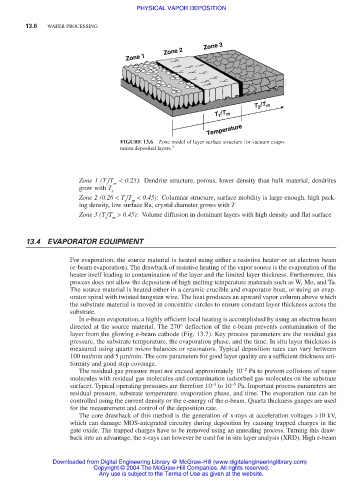
FIGURE 13.6 Zone model of layer surface structure for vacuum evapo-
ration deposited layers. 3
Zone 1 (T /T < 0.25): Dendrite structure, porous, lower density than bulk material, dendrites
s m
grow with T
s
Zone 2 (0.26 < T /T < 0.45): Columnar structure, surface mobility is large enough, high pack-
s m
ing density, low surface Ra, crystal diameter grows with T
Zone 3 (T /T > 0.45): Volume diffusion in dominant layers with high density and flat surface
s m
13.4 EVAPORATOR EQUIPMENT
For evaporation, the source material is heated using either a resistive heater or an electron beam
(e-beam evaporation). The drawback of resistive heating of the vapor source is the evaporation of the
heater itself leading to contamination of the layer and the limited layer thickness. Furthermore, this
process does not allow the deposition of high melting temperature materials such as W, Mo, and Ta.
The source material is heated either in a ceramic crucible and evaporator boat, or using an evap-
orator spiral with twisted tungsten wire. The heat produces an upward vapor column above which
the substrate material is moved in concentric circles to ensure constant layer thickness across the
substrate.
In e-beam evaporation, a highly efficient local heating is accomplished by using an electron beam
directed at the source material. The 270° deflection of the e-beam prevents contamination of the
layer from the glowing e-beam cathode (Fig. 13.7). Key process parameters are the residual gas
pressure, the substrate temperature, the evaporation phase, and the time. In situ layer thickness is
measured using quartz micro balances or resonators. Typical deposition rates can vary between
100 nm/min and 5 µm/min. The core parameters for good layer quality are a sufficient thickness uni-
formity and good step coverage.
−2
The residual gas pressure must not exceed approximately 10 Pa to prevent collisions of vapor
molecules with residual gas molecules and contamination (adsorbed gas molecules on the substrate
−5
−3
surface). Typical operating pressures are therefore 10 to 10 Pa. Important process parameters are
residual pressure, substrate temperature, evaporation phase, and time. The evaporation rate can be
controlled using the current density or the e-energy of the e-beam. Quartz thickness gauges are used
for the measurement and control of the deposition rate.
The core drawback of this method is the generation of x-rays at acceleration voltages >10 kV,
which can damage MOS-integrated circuitry during deposition by causing trapped charges in the
gate oxide. The trapped charges have to be removed using an annealing process. Turning this draw-
back into an advantage, the x-rays can however be used for in situ layer analysis (XRD). High e-beam
Downloaded from Digital Engineering Library @ McGraw-Hill (www.digitalengineeringlibrary.com)
Copyright © 2004 The McGraw-Hill Companies. All rights reserved.
Any use is subject to the Terms of Use as given at the website.