
Page 186 - Semiconductor Manufacturing Handbook
P. 186
Geng(SMH)_CH13.qxd 04/04/2005 19:51 Page 13.9
PHYSICAL VAPOR DEPOSITION
PHYSICAL VAPOR DEPOSITION 13.9
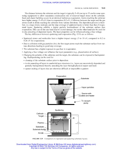
The distance between the substrate and the target is typically 5–10 cm (up to 35 cm for some sput-
tering equipment) to allow maximum condensation rate of removed target atoms on the substrate.
Seed and cluster building occurs in an identical fashion as evaporation. Atoms reaching the substrate
have higher energy (3–10 eV) than in evaporation (0.2 eV). Collisions between the target and the gas
atoms result in atoms reaching the substrate from various directions. The deposition process is there-
fore, to a large extent, isotropic and the step coverage of sputtered layers is better than that of evapo-
rated layers. Sputtering exhibits a higher particle bombardment of the substrate surface than
evaporation. This can on the one hand lead to crystal damage, but on the other hand also be used for
in situ annealing of deposited layers. The layer properties can be influenced using a bias voltage.
The key differences between sputtering and evaporation (Fig. 13.9) are as follows:
• Sputtered atoms and molecules have a higher impact energy (3 to 10 eV, compared to 0.2 to
0.26 eV for evaporation).
• Due to collisions with gas particles (Ar), the free target atoms reach the substrate surface from var-
ious directions leading to good step coverage.
• The substrate has a higher exposure to gas than in evaporation.
• Applying a bias voltage can influence the layer parameters (e.g., planarisation of surface).
• Changing the polarity of the substrate and the target, the substrate can be exposed to backsputter-
ing. Backsputtering can be used for
cleaning of the substrate surface prior to deposition
in situ annealing of layers in sandwich layer structures (i.e., layers are successively deposited and
partially backsputtered thereby annealing the layer through physical impact and heat)
sputter etching of layers that are otherwise difficult or impossible to pattern
Evaporation
Substrate
Vapor particles
Source with
crucible and heater
To vacuum
pump
Sputtering
Cathode
Target −
e − Metal, e.g., Al
Ar
Plasma
Ar +
Substrate
Substrate holder
Al
+
Anode
FIGURE 13.9 Comparison of evaporation and sputtering (schematic layout).
Downloaded from Digital Engineering Library @ McGraw-Hill (www.digitalengineeringlibrary.com)
Copyright © 2004 The McGraw-Hill Companies. All rights reserved.
Any use is subject to the Terms of Use as given at the website.