Page 193 - Semiconductor Manufacturing Handbook
P. 193

Geng(SMH)_CH13.qxd  05/04/2005  18:03  Page 13.16


                                                 PHYSICAL VAPOR DEPOSITION

                   13.16  WAFER PROCESSING

                                                            Cathode

                                               (a)      M O                      Target


                                               (b)          M O


                                               (c)
                                                                     M O        Substrate

                                                             Anode
                                               FIGURE 13.19  Schematic and reaction sites for reactive sput-
                                               tering. 1


                               charge the customer only for the extra material as well as the sintering and bonding of the new tar-
                               get material (Figs. 13.21 and 13.22).

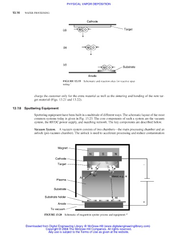
                   13.7.8 Sputtering Equipment

                               Sputtering equipment have been built in a multitude of different ways. The schematic layout of the most
                               common systems today is given in Fig. 13.23. The core components of such a system are the vacuum
                               system, the RF/DC power supply, and matching network. The key components are described below.
                               Vacuum System. A vacuum system consists of two chambers—the main processing chamber and an
                               airlock (pre-vacuum chamber). The airlock is used to accelerate processing and reduce contamination


                                            Magnet
                                                             N       S     N
                                           Cathode
                                            Target                                         −
                                                            e −
                                                               Ar  +      Metal, e.g., Al
                                                        Ar
                                           Plasma

                                          Substrate

                                     Substrate holder                       Al
                                                                                           +
                                            Anode
                                        To vacuum
                                     FIGURE 13.20  Schematic of magnetron sputter process and equipment. 12


                          Downloaded from Digital Engineering Library @ McGraw-Hill (www.digitalengineeringlibrary.com)
                                     Copyright © 2004 The McGraw-Hill Companies. All rights reserved.
                                       Any use is subject to the Terms of Use as given at the website.
   188   189   190   191   192   193   194   195   196   197   198