
Page 198 - Semiconductor Manufacturing Handbook
P. 198
Geng(SMH)_CH13.qxd 04/04/2005 19:51 Page 13.21
PHYSICAL VAPOR DEPOSITION
PHYSICAL VAPOR DEPOSITION 13.21
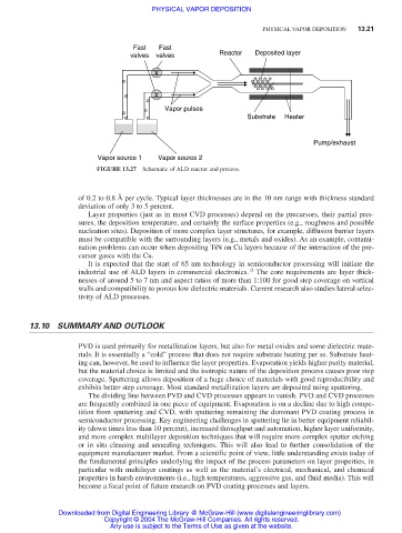
Fast Fast
Reactor Deposited layer
valves valves
X
X
Vapor pulses
Substrate Heater
Pump/exhaust
Vapor source 1 Vapor source 2
FIGURE 13.27 Schematic of ALD reactor and process.
of 0.2 to 0.8 Å per cycle. Typical layer thicknesses are in the 10 nm range with thickness standard
deviation of only 3 to 5 percent.
Layer properties (just as in most CVD processes) depend on the precursors, their partial pres-
sures, the deposition temperature, and certainly the surface properties (e.g., roughness and possible
nucleation sites). Deposition of more complex layer structures, for example, diffusion barrier layers
must be compatible with the surrounding layers (e.g., metals and oxides). As an example, contami-
nation problems can occur when depositing TiN on Cu layers because of the interaction of the pre-
cursor gases with the Cu.
It is expected that the start of 65 nm technology in semiconductor processing will initiate the
industrial use of ALD layers in commercial electronics. 12 The core requirements are layer thick-
nesses of around 5 to 7 nm and aspect ratios of more than 1:100 for good step coverage on vertical
walls and compatibility to porous low dielectric materials. Current research also studies lateral selec-
tivity of ALD processes.
13.10 SUMMARY AND OUTLOOK
PVD is used primarily for metallization layers, but also for metal oxides and some dielectric mate-
rials. It is essentially a “cold” process that does not require substrate heating per se. Substrate heat-
ing can, however, be used to influence the layer properties. Evaporation yields higher purity material,
but the material choice is limited and the isotropic nature of the deposition process causes poor step
coverage. Sputtering allows deposition of a huge choice of materials with good reproducibility and
exhibits better step coverage. Most standard metallization layers are deposited using sputtering.
The dividing line between PVD and CVD processes appears to vanish. PVD and CVD processes
are frequently combined in one piece of equipment. Evaporation is on a decline due to high compe-
tition from sputtering and CVD, with sputtering remaining the dominant PVD coating process in
semiconductor processing. Key engineering challenges in sputtering lie in better equipment reliabil-
ity (down times less than 10 percent), increased throughput and automation, higher layer uniformity,
and more complex multilayer deposition techniques that will require more complex sputter etching
or in situ cleaning and annealing techniques. This will also lead to further consolidation of the
equipment manufacturer market. From a scientific point of view, little understanding exists today of
the fundamental principles underlying the impact of the process parameters on layer properties, in
particular with multilayer coatings as well as the material’s electrical, mechanical, and chemical
properties in harsh environments (i.e., high temperatures, aggressive gas, and fluid media). This will
become a focal point of future research on PVD coating processes and layers.
Downloaded from Digital Engineering Library @ McGraw-Hill (www.digitalengineeringlibrary.com)
Copyright © 2004 The McGraw-Hill Companies. All rights reserved.
Any use is subject to the Terms of Use as given at the website.