
Page 197 - Semiconductor Manufacturing Handbook
P. 197
Geng(SMH)_CH13.qxd 04/04/2005 19:51 Page 13.20
PHYSICAL VAPOR DEPOSITION
13.20 WAFER PROCESSING
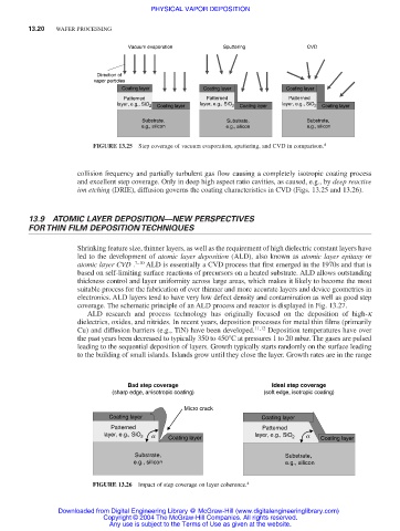
Vacuum evaporation Sputtering CVD
Direction of
vapor particles
Coating layer Coating layer Coating layer
Patterned Patterned Patterned
layer, e.g., SiO 2 Coating layer layer, e.g., SiO 2 Coating layer layer, e.g., SiO 2 Coating layer
Substrate, Substrate, Substrate,
e.g., silicon e.g., silicon e.g., silicon
FIGURE 13.25 Step coverage of vacuum evaporation, sputtering, and CVD in comparison. 4
collision frequency and partially turbulent gas flow causing a completely isotropic coating process
and excellent step coverage. Only in deep high aspect ratio cavities, as caused, e.g., by deep reactive
ion etching (DRIE), diffusion governs the coating characteristics in CVD (Figs. 13.25 and 13.26).
13.9 ATOMIC LAYER DEPOSITION––NEW PERSPECTIVES
FOR THIN FILM DEPOSITION TECHNIQUES
Shrinking feature size, thinner layers, as well as the requirement of high dielectric constant layers have
led to the development of atomic layer deposition (ALD), also known as atomic layer epitaxy or
atomic layer CVD . 7–10 ALD is essentially a CVD process that first emerged in the 1970s and that is
based on self-limiting surface reactions of precursors on a heated substrate. ALD allows outstanding
thickness control and layer uniformity across large areas, which makes it likely to become the most
suitable process for the fabrication of ever thinner and more accurate layers and device geometries in
electronics. ALD layers tend to have very low defect density and contamination as well as good step
coverage. The schematic principle of an ALD process and reactor is displayed in Fig. 13.27.
ALD research and process technology has originally focused on the deposition of high-k
dielectrics, oxides, and nitrides. In recent years, deposition processes for metal thin films (primarily
Cu) and diffusion barriers (e.g., TiN) have been developed. 11,12 Deposition temperatures have over
the past years been decreased to typically 350 to 450°C at pressures 1 to 20 mbar. The gases are pulsed
leading to the sequential deposition of layers. Growth typically starts randomly on the surface leading
to the building of small islands. Islands grow until they close the layer. Growth rates are in the range
Bad step coverage Ideal step coverage
(sharp edge, anisotropic coating) (soft edge, isotropic coating)
Micro crack
Coating layer Coating layer
Patterned Patterned
layer, e.g., SiO 2 a Coating layer layer, e.g., SiO 2 a Coating layer
Substrate, Substrate,
e.g., silicon e.g., silicon
FIGURE 13.26 Impact of step coverage on layer coherence. 4
Downloaded from Digital Engineering Library @ McGraw-Hill (www.digitalengineeringlibrary.com)
Copyright © 2004 The McGraw-Hill Companies. All rights reserved.
Any use is subject to the Terms of Use as given at the website.