
Page 217 - Semiconductor Manufacturing Handbook
P. 217
Geng(SMH)_CH15.qxd 04/04/2005 19:53 Page 15.2
EPITAXY
15.2 WAFER PROCESSING
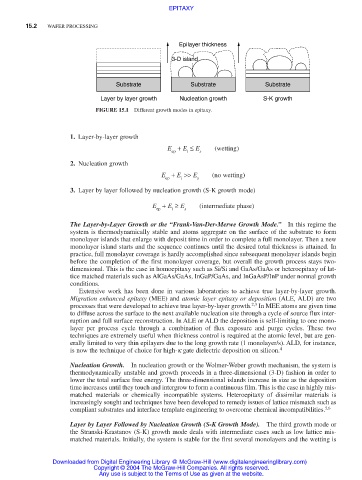
Epilayer thickness
3-D island
Substrate Substrate Substrate
Layer by layer growth Nucleation growth S-K growth
FIGURE 15.1 Different growth modes in epitaxy.
1. Layer-by-layer growth
E + E ≤ E (wetting)
ep i s
2. Nucleation growth
E + E >> E (no wetting)
ep i s
3. Layer by layer followed by nucleation growth (S-K growth mode)
E + E ≥ E (intermediate phase)
ep i s
The Layer-by-Layer Growth or the “Frank-Van-Der-Merwe Growth Mode.” In this regime the
system is thermodynamically stable and atoms aggregate on the surface of the substrate to form
monolayer islands that enlarge with deposit time in order to complete a full monolayer. Then a new
monolayer island starts and the sequence continues until the desired total thickness is attained. In
practice, full monolayer coverage is hardly accomplished since subsequent monolayer islands begin
before the completion of the first monolayer coverage, but overall the growth process stays two-
dimensional. This is the case in homoepitaxy such as Si/Si and GaAs/GaAs or heteroepitaxy of lat-
tice matched materials such as AlGaAs/GaAs, InGaP/GaAs, and InGaAsP/InP under normal growth
conditions.
Extensive work has been done in various laboratories to achieve true layer-by-layer growth.
Migration enhanced epitaxy (MEE) and atomic layer epitaxy or deposition (ALE, ALD) are two
processes that were developed to achieve true layer-by-layer growth. 2,3 In MEE atoms are given time
to diffuse across the surface to the next available nucleation site through a cycle of source flux inter-
ruption and full surface reconstruction. In ALE or ALD the deposition is self-limiting to one mono-
layer per process cycle through a combination of flux exposure and purge cycles. These two
techniques are extremely useful when thickness control is required at the atomic level, but are gen-
erally limited to very thin epilayers due to the long growth rate (1 monolayer/s). ALD, for instance,
is now the technique of choice for high-k gate dielectric deposition on silicon. 4
Nucleation Growth. In nucleation growth or the Wolmer-Weber growth mechanism, the system is
thermodynamically unstable and growth proceeds in a three-dimensional (3-D) fashion in order to
lower the total surface free energy. The three-dimensional islands increase in size as the deposition
time increases until they touch and intergrow to form a continuous film. This is the case in highly mis-
matched materials or chemically incompatible systems. Heteroepitaxy of dissimilar materials is
increasingly sought and techniques have been developed to remedy issues of lattice mismatch such as
compliant substrates and interface template engineering to overcome chemical incompatibilities. 5,6
Layer by Layer Followed by Nucleation Growth (S-K Growth Mode). The third growth mode or
the Stranski-Krastanov (S-K) growth mode deals with intermediate cases such as low lattice mis-
matched materials. Initially, the system is stable for the first several monolayers and the wetting is
Downloaded from Digital Engineering Library @ McGraw-Hill (www.digitalengineeringlibrary.com)
Copyright © 2004 The McGraw-Hill Companies. All rights reserved.
Any use is subject to the Terms of Use as given at the website.