
Page 220 - Semiconductor Manufacturing Handbook
P. 220
Geng(SMH)_CH15.qxd 04/04/2005 19:53 Page 15.5
EPITAXY
EPITAXY 15.5
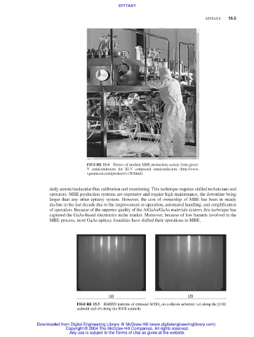
FIGURE 15.4 Picture of modern MBE production system from group-
V semiconductors for III-V compound semiconductors (http://www.
vgsemicon.com/products/v150.html).
daily atomic/molecular flux calibration and monitoring. This technique requires skilled technicians and
operators. MBE production systems are expensive and require high maintenance, the downtime being
larger than any other epitaxy system. However, the cost of ownership of MBE has been in steady
decline in the last decade due to the improvement in operation, automated handling, and simplification
of operation. Because of the superior quality of the AlGaAs/GaAs materials system, this technique has
captured the GaAs-based electronics niche market. Moreover, because of low hazards involved in the
MBE process, most GaAs epitaxy foundries have shifted their operations to MBE.
FIGURE 15.5 RHEED patterns of epitaxial SrTiO on a silicon substrate: (a) along the [110]
3
azimuth and (b) along the [010] azimuth.
Downloaded from Digital Engineering Library @ McGraw-Hill (www.digitalengineeringlibrary.com)
Copyright © 2004 The McGraw-Hill Companies. All rights reserved.
Any use is subject to the Terms of Use as given at the website.