
Page 218 - Semiconductor Manufacturing Handbook
P. 218
Geng(SMH)_CH15.qxd 04/04/2005 19:53 Page 15.3
EPITAXY
EPITAXY 15.3
complete. As the thickness increases, the total surface free energy increases, and a breakdown occurs
followed by a three-dimensional growth. Pseudomorphic structures such as GaInAs/GaAs and
SiGe/Si are a few examples where the S-K mode growth process is applied.
15.1.2 Growth Techniques and Equipment
Varieties of methods are used to grow crystalline materials on crystalline substrates. In the semi-
conductor industry two major techniques are well established—chemical vapor deposition (CVD)
and molecular beam epitaxy (MBE). Both techniques are of nonequilibrium character. Variants of
these techniques—metal-organic chemical vapor deposition (MOCVD)—are associated with the
epitaxy of compound semiconductors arsenides-, phosphides-, and nitrides-based materials, and
chemical beam epitaxy (CBE) or gas source MBE (GSMBE) where the elemental sources are
gaseous instead of solid sources. A combination of CVD and ultrahigh vacuum deposition system
(UHV-CVD) is generating acceptance in some applications such as the SiGe/Si materials system. 7
15.1.3 Molecular Beam Epitaxy
8
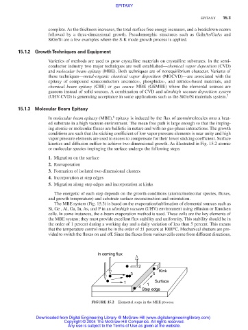
In molecular beam epitaxy (MBE), epitaxy is induced by the flux of atoms/molecules onto a heat-
ed substrate in a high vacuum environment. The mean free path is large enough so that the imping-
ing atomic or molecular fluxes are ballistic in nature and with no gas-phase interactions. The growth
conditions are such that the sticking coefficient of low vapor pressure elements is near unity and high
vapor pressure elements are used in excess to compensate for their lower sticking coefficient. Surface
kinetics and diffusion suffice to achieve two-dimensional growth. As illustrated in Fig. 15.2 atomic
or molecular species impinging the surface undergo the following steps:
1. Migration on the surface
2. Reevaporation
3. Formation of isolated two-dimensional clusters
4. Incorporation at step edges
5. Migration along step edges and incorporation at kinks
The energetic of each step depends on the growth conditions (atomic/molecular species, fluxes,
and growth temperature) and substrate surface reconstruction and orientation.
The MBE system (Fig. 15.3) is based on the evaporation/sublimation of elemental sources such as
Si, Ge , Al, Ga, In, As, and P in an ultrahigh vacuum (UHV) environment using effusion or Knudsen
cells. In some instances, the e-beam evaporation method is used. These cells are the key elements of
the MBE system; they must provide excellent flux stability and uniformity. This stability should be in
the order of 1 percent during a working day and a daily variation of less than 5 percent. This means
that the temperature control must be in the order of ±1 percent at 1000°C. Mechanical shutters are pro-
vided to switch the fluxes on and off. Since the fluxes from various cells come from different directions,
In coming flux
2
Kink
3 5
1 1 Surface
4
Step edge
FIGURE 15.2 Elemental steps in the MBE process.
Downloaded from Digital Engineering Library @ McGraw-Hill (www.digitalengineeringlibrary.com)
Copyright © 2004 The McGraw-Hill Companies. All rights reserved.
Any use is subject to the Terms of Use as given at the website.