
Page 225 - Semiconductor Manufacturing Handbook
P. 225
Geng(SMH)_CH15.qxd 04/04/2005 19:53 Page 15.10
EPITAXY
15.10 WAFER PROCESSING
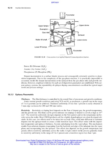
Pyrometer
Upper lamps Upper dome
Susceptor
Gas inlet
Exhaust
Wafer lift shaft Lower dome
Lower IR lamps
Pyrometer
FIGURE 15.10 Cross section of an Applied Material Centura deposition chamber.
Boron (B) Diborane (B H )
2 6
Arsenic (As) Arsine (AsH )
3
Phosphorous (P) Phosphine (PH )
3
Dopant incorporation is a surface kinetic process and consequently extremely sensitive to depo-
sition temperature. Due to the complexity of the gas-phase reaction, it is practically impossible to
accurately model the dopant incorporation in the epilayer from the gas-phase ratio and growth con-
ditions. However, empirical solutions for each set of deposition parameters are established. With cur-
rent epitaxy systems, the repeatability of epilayer doping concentration is excellent for typical target
levels and process settings.
15.2.2 Epitaxy Parametric
Thickness. The film thickness is controlled by the overall flow of precursors and growth conditions.
Under normal growth conditions and using TCS and H as precursors, a growth rate in the range
2
of 3 to 4 µm/min can be achieved. Thickness uniformity of less that 1 percent is easily obtained at
3 mm edge exclusion for 200 and 300 mm wafers.
Resistivity. Resistivity or doping level depends on the flow of dopant gas, the growth temperature,
and the growth rate. The films can be grown intrinsic (no doping) or doped to a level as high as 10 19
3
/cm . The resistivity uniformity strongly depends on the flow pattern and on the temperature unifor-
mity across the wafer. Most CMOS products call for a lightly doped epilayer on a heavily doped sub-
strate. In this case, two effects need to be taken into account. First, solid state diffusion of substrate
dopants into the epilayer tends to create a wide transition layer. This effect varies with the deposi-
tion temperature and epilayer thickness. Second, autodoping from the vapor phase. This mechanism
results from substrate dopants evaporating from the backside and edge of the substrate into the vapor
phase and incorporating into the epilayer. This effect also depends on the growth temperature and
greatly affects resistivity uniformity across the wafer. A tight control on the process generally leads
to resistivity uniformity in the range of 2 to 4 percent and a transition region less than 1 µm.
Downloaded from Digital Engineering Library @ McGraw-Hill (www.digitalengineeringlibrary.com)
Copyright © 2004 The McGraw-Hill Companies. All rights reserved.
Any use is subject to the Terms of Use as given at the website.