
Page 226 - Semiconductor Manufacturing Handbook
P. 226
Geng(SMH)_CH15.qxd 04/04/2005 19:53 Page 15.11
EPITAXY
EPITAXY 15.11
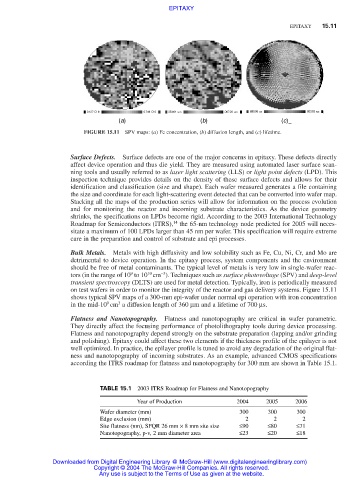
(a) (b) (c)
FIGURE 15.11 SPV maps: (a) Fe concentration, (b) diffusion length, and (c) lifetime.
Surface Defects. Surface defects are one of the major concerns in epitaxy. These defects directly
affect device operation and thus die yield. They are measured using automated laser surface scan-
ning tools and usually referred to as laser light scattering (LLS) or light point defects (LPD). This
inspection technique provides details on the density of these surface defects and allows for their
identification and classification (size and shape). Each wafer measured generates a file containing
the size and coordinate for each light-scattering event detected that can be converted into wafer map.
Stacking all the maps of the production series will allow for information on the process evolution
and for monitoring the reactor and incoming substrate characteristics. As the device geometry
shrinks, the specifications on LPDs become rigid. According to the 2003 International Technology
14
Roadmap for Semiconductors (ITRS), the 65-nm technology node predicted for 2005 will neces-
sitate a maximum of 100 LPDs larger than 45 nm per wafer. This specification will require extreme
care in the preparation and control of substrate and epi processes.
Bulk Metals. Metals with high diffusivity and low solubility such as Fe, Cu, Ni, Cr, and Mo are
detrimental to device operation. In the epitaxy process, system components and the environment
should be free of metal contaminants. The typical level of metals is very low in single-wafer reac-
−3
10
9
tors (in the range of 10 to 10 cm ). Techniques such as surface photovoltage (SPV) and deep-level
transient spectroscopy (DLTS) are used for metal detection. Typically, iron is periodically measured
on test wafers in order to monitor the integrity of the reactor and gas delivery systems. Figure 15.11
shows typical SPV maps of a 300-mm epi-wafer under normal epi operation with iron concentration
9
in the mid-10 cm a diffusion length of 360 µm and a lifetime of 700 µs.
3
Flatness and Nanotopography. Flatness and nanotopography are critical in wafer parametric.
They directly affect the focusing performance of photolithography tools during device processing.
Flatness and nanotopography depend strongly on the substrate preparation (lapping and/or grinding
and polishing). Epitaxy could affect these two elements if the thickness profile of the epilayer is not
well optimized. In practice, the epilayer profile is tuned to avoid any degradation of the original flat-
ness and nanotopography of incoming substrates. As an example, advanced CMOS specifications
according the ITRS roadmap for flatness and nanotopography for 300 mm are shown in Table 15.1.
TABLE 15.1 2003 ITRS Roadmap for Flatness and Nanotopography
Year of Production 2004 2005 2006
Wafer diameter (mm) 300 300 300
Edge exclusion (mm) 2 2 2
Site flatness (nm), SFQR 26 mm × 8 mm site size ≤90 ≤80 ≤71
Nanotopography, p-v, 2 mm diameter area ≤23 ≤20 ≤18
Downloaded from Digital Engineering Library @ McGraw-Hill (www.digitalengineeringlibrary.com)
Copyright © 2004 The McGraw-Hill Companies. All rights reserved.
Any use is subject to the Terms of Use as given at the website.