
Page 227 - Semiconductor Manufacturing Handbook
P. 227
Geng(SMH)_CH15.qxd 04/04/2005 19:53 Page 15.12
EPITAXY
15.12 WAFER PROCESSING
However, customer requirements are often one to two generations ahead of the general trend and
pressurize the epitaxial wafer producers to develop products at a greater pace than the customer
requirements. R&D epitaxy laboratories have already produced epitaxial wafers with state-of-the-art
flatness, nanotopography, and LPDs.
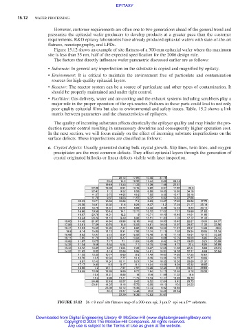
Figure 15.12 shows an example of site flatness of a 300-mm epitaxial wafer where the maximum
site is less than 35 nm, half of the expected specification for the 2006 design rule.
The factors that directly influence wafer parametric discussed earlier are as follows:
• Substrate: In general any imperfection on the substrate is copied and magnified by epitaxy.
• Environment: It is critical to maintain the environment free of particulate and contamination
sources for high-quality epitaxial layers.
• Reactor: The reactor system can be a source of particulate and other types of contamination. It
should be properly maintained and under tight control.
• Facilities: Gas delivery, water and air-cooling and the exhaust systems including scrubbers play a
major role in the proper operation of the epi-reactor. Failures in these parts could lead to not only
poor quality epitaxial films but also to environmental and safety issues. Table. 15.2 shows a link
matrix between parameters and the characteristics of epilayers.
The quality of incoming substrates affects drastically the epilayer quality and may hinder the pro-
duction reactor control resulting in unnecessary downtime and consequently higher operation cost.
In the next section, we will focus mainly on the effect of incoming substrate imperfections on the
surface defects. These imperfections are classified as follows:
a. Crystal defects: Usually generated during bulk crystal growth. Slip lines, twin lines, and oxygen
precipitates are the most common defects. They affect epitaxial layers through the generation of
crystal originated hillocks or linear defects visible with laser inspection.
26.12 17.85 10.48 31.78
23.6 14.2 10.32 11.44 9.66 28.14
19.49 11.53 11.33 11.26 7.46 22.67
22.96 13.08 6.84 13.15 9.92 8.07 17.82 26.6
22.47 11.2 9.52 8.93 6.88 10.85 15.95 34.16
11.07 9.75 14.02 10.6 7.52 8.35 15.47 28.16
11.78 9.67 14.63 11.57 9.72 9.02 14.42 27.66
25.33 10.71 10.69 10.68 7.3 9.69 13.07 17.83 26.56 17.75
23.56 14.81 12.32 11.8 8.29 8.07 11.2 17.24 21.17 25.18
18.69 14.76 11.31 13.72 8.06 15.58 9.88 15.16 9.23 24.11
16.66 19.58 10.45 14.1 12.71 15.12 17.02 11.7 13.69 21.03
18.07 23.76 11.51 12.2 9 10.71 19.49 10.49 14.01 11.86
18.34 20.28 11.12 9.49 8.96 15.51 11.83 7.78 17.72 11.43
18.83 14.42 21.97 14.94 13.99 12.16 14.2 10.93 13.43 22.27 13.31 24.77
17.89 13.01 17.69 10.76 14.8 10.06 14.61 10.04 12.97 20.87 11.33 22.56
16.41 12.04 15.59 14.04 7.37 8.82 14.86 13.02 11.91 20.07 14.36 28.5
18.8 6.14 15.83 11.12 8.31 7.92 13.74 11.19 7.53 23.24 10.95 31.18
16.69 9.03 10.97 5.72 8.54 15.82 16.48 9.76 11.79 15.07 10.12 23.03
18.11 7.95 11.79 8.07 8.47 13.94 13.94 9.68 15.79 16.03 6.85 29.44
10.69 11.07 10.75 7.17 7.1 11.64 19.45 8.42 14.27 19.65 8.21 33.99
14.35 11.24 9.56 8.54 5.54 7.1 15.75 12.95 9.72 22.4 6.85 36.69
15.43 12.72 10.09 8.07 11.04 7.35 16.27 12.06 11.68 22.31 5.69 28.74
14.52 21.02 8.82 8.19 10.88 9.95 15.61 10.81 16.38 22.27 6.04 30.84
11.25 10.09 10.74 6.65 8.6 11.49 16.02 14.93 17.55 12.61
10.76 12.5 12.34 7.77 10.1 8.16 13.36 13.75 15.77 19.09
9.67 12.42 11.31 10.11 6.21 7.54 10.35 10.53 20.89 21.37
17.17 9.49 9.3 9.17 8.1 11.04 13.36 8.04 15.32 18.85
18.66 7.2 12.11 7.97 7.97 10.48 12.45 8.9 10.57 29.69
18.55 10.66 13.26 9.69 9.77 7.94 14.13 12.55 8.16 23.33
10.4 11.21 8.89 14 11.6 11.99 11.32 16.6
12.3 9.98 11.41 11.75 13.13 14.47 13.93 26.73
24.46 12.49 10.57 9.45 9.52 12.64 9.43 29.75
23.41 11.25 9.16 15.72 9.08 10.13 15.6 24.22
23.39 10.12 15.45 12.73 9.92 18.65
22.2 13.27 14.49 12.2 10.62 22.24
22.29 16.38 10.63 24.61
−
++
2
FIGURE 15.12 26 × 8 mm site flatness map of a 300-mm epi; 3 µm P epi on a P substrate.
Downloaded from Digital Engineering Library @ McGraw-Hill (www.digitalengineeringlibrary.com)
Copyright © 2004 The McGraw-Hill Companies. All rights reserved.
Any use is subject to the Terms of Use as given at the website.