
Page 6 - Semiconductor Manufacturing Handbook
P. 6
Geng(SMH)_CH01.qxd 05/04/2005 18:01 Page 1.5
HOW SEMICONDUCTOR CHIPS ARE MADE
HOW SEMICONDUCTOR CHIPS ARE MADE 1.5
1.5 WHERE CHIPS ARE MADE
Chips are made in the most sophisticated manufacturing plants in the world, called wafer fabrication
facilities or wafer fab. Typically 300-mm fabs cost $2 billion to build and equip. Today, there are
over 1000 fabs around the world producing millions of chips everyday.
The chip manufacturing process occurs in a cleanroom of a fab. A class-one cleanroom provides
the world’s cleanest environment where air is continuously filtered to keep airborne contaminants to
not more than one dust per cubic foot. Huge air filtration systems completely change the air in the
cleanroom at the rate of about 10 times per minute. In addition to the cleanest air, stringent cleanli-
ness requirements are also followed in the use of chip-making materials, chemicals, and processing
equipment. Workers in fabs wear special clothing including gowns called “bunny suits,” hoods, face-
masks, glasses, gloves, and shoe covers to avoid contaminating the chips. The temperature, baro-
metric pressure, and humidity are controlled. All these efforts to avoid contamination in fabs are
needed to ensure an accepted yield of chips that meet specifications.
1.6 HOW CHIPS ARE MADE
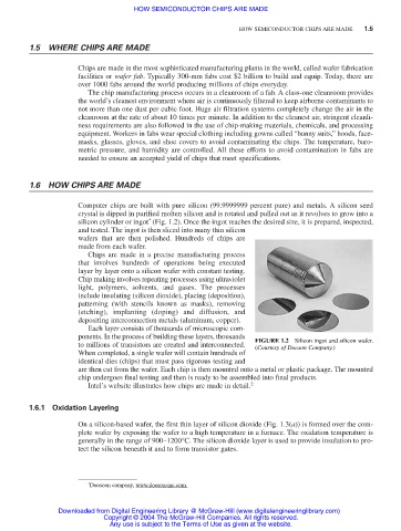
Computer chips are built with pure silicon (99.9999999 percent pure) and metals. A silicon seed
crystal is dipped in purified molten silicon and is rotated and pulled out as it revolves to grow into a
*
silicon cylinder or ingot (Fig. 1.2). Once the ingot reaches the desired size, it is prepared, inspected,
and tested. The ingot is then sliced into many thin silicon
wafers that are then polished. Hundreds of chips are
made from each wafer.
Chips are made in a precise manufacturing process
that involves hundreds of operations being executed
layer by layer onto a silicon wafer with constant testing.
Chip making involves repeating processes using ultraviolet
light, polymers, solvents, and gases. The processes
include insulating (silicon dioxide), placing (deposition),
patterning (with stencils known as masks), removing
(etching), implanting (doping) and diffusion, and
depositing interconnection metals (aluminum, copper).
Each layer consists of thousands of microscopic com-
ponents. In the process of building these layers, thousands FIGURE 1.2 Silicon ingot and silicon wafer.
to millions of transistors are created and interconnected.
(Courtesy of Dooson Company.)
When completed, a single wafer will contain hundreds of
identical dies (chips) that must pass rigorous testing and
are then cut from the wafer. Each chip is then mounted onto a metal or plastic package. The mounted
chip undergoes final testing and then is ready to be assembled into final products.
Intel’s website illustrates how chips are made in detail. 2
1.6.1 Oxidation Layering
On a silicon-based wafer, the first thin layer of silicon dioxide (Fig. 1.3(a)) is formed over the com-
plete wafer by exposing the wafer to a high temperature in a furnace. The oxidation temperature is
generally in the range of 900–1200°C. The silicon dioxide layer is used to provide insulation to pro-
tect the silicon beneath it and to form transistor gates.
* Doosoon company, www.dooson-inc.com.
Downloaded from Digital Engineering Library @ McGraw-Hill (www.digitalengineeringlibrary.com)
Copyright © 2004 The McGraw-Hill Companies. All rights reserved.
Any use is subject to the Terms of Use as given at the website.