
Page 8 - Semiconductor Manufacturing Handbook
P. 8
Geng(SMH)_CH01.qxd 04/04/2005 19:32 Page 1.7
HOW SEMICONDUCTOR CHIPS ARE MADE
HOW SEMICONDUCTOR CHIPS ARE MADE 1.7
Photoresist Photoresist
SiO
SiO 2 2
Si-substrate
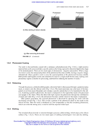
(f) After etching of silicon dioxide
SiO 2 SiO 2
Si-substrate
(g) After removing photoresist
FIGURE 1.3 (Continued)
1.6.2 Photoresist Coating
The wafer is then uniformly coated with a substance called photoresist (Fig. 1.3(b)), a light-sensitive
material that can be processed into a specific pattern after being exposed to ultraviolet light in the shape
of the desired pattern. There are two main types of photoresists—negative and positive. When a nega-
tive resist is used, the unexposed portion of the photoresist becomes soluble, leaving a negative image.
Alternatively when a positive resist is used, the exposed portion of the photoresist becomes soluble.
Both positive and negative resists can sometimes be used on a single mask for two steps, making com-
plementary regions available for processing, and therefore reducing the number of masks. 3
1.6.3 Patterning
Through the process called photolithography, ultraviolet light is then passed through a patterned glass
mask, or stencil, onto the silicon wafer (Fig. 1.3(c)). The mask represents one color layer of the inte-
grated circuit from mask blueprints and contains a specific pattern that is to be transferred to the sili-
con. Assuming a positive photoresist, the mask is transparent in the region that needs to be processed
and opaque in the others. When the ultraviolet light exposes the photoresist through the combination
of mask and wafer (Fig. 1.3(d)), the photoresist becomes soluble wherever the mask is transparent.
After pattern generation, the exposed photoresist is dissolved by spraying the wafer with the
developing solvent (Fig. 1.3(e)). This reveals a pattern of the photoresist made by the mask on the
silicon dioxide. Then the wafer is hardened at a low temperature so that the remaining photoresist,
which can resist the strong acid, is used to etch the exposed oxide layer.
1.6.4 Etching
The revealed silicon dioxide is removed through a process called etching, which stops at the silicon
surface (Fig. 1.3( f )). There are two main types of etching technologies—wet and dry etching.
Downloaded from Digital Engineering Library @ McGraw-Hill (www.digitalengineeringlibrary.com)
Copyright © 2004 The McGraw-Hill Companies. All rights reserved.
Any use is subject to the Terms of Use as given at the website.