
Page 12 - Semiconductor Manufacturing Handbook
P. 12
Geng(SMH)_CH01.qxd 04/04/2005 19:32 Page 1.11
HOW SEMICONDUCTOR CHIPS ARE MADE
HOW SEMICONDUCTOR CHIPS ARE MADE 1.11
1.6.7 Depositing Interconnection Metals
To connect different layers, similar layering and patterning processes are repeated (Fig. 1.6(a)–(c)).
A mask is used to define contact holes allowing for the connections to be made between layers. After
the etching of the silicon dioxide in the exposed area (Fig. 1.6(d)) and the removal of the remaining
photoresist (Fig. 1.6(e)), the contact holes are created. A combination of tungsten and aluminum is
then deposited onto the whole wafer to fill the contact holes under high-vacuum conditions (Fig.
1.6(f)). Another patterning and etching stage defines a contact pattern and leaves strips of the metal
to make the electrical connections (Fig. 1.6(g)). In sophisticated circuits, the interconnect wiring is
so complex that it is impossible to complete within a single layer.
Approximately 20 layers are connected to form an IC in a three-dimensional structure. The
exact number of layers on a wafer depends on the complexity of the design. After all the desired
levels are in place, a final layer of insulation is deposited to protect the fragile aluminum wiring.
In the last photolithograph step, small pads along the edge of the microchip are left exposed. These
aluminum pads are the contact points between the microscopic wiring of the IC and the outside
world.
1.6.8 Testing
In the previous example a simplified process is completed to manufacture a tiny portion of a
microchip. In reality, making a chip is much more complex. The complete run of the manufacturing
process might involve hundreds of individual steps and take weeks to complete. Identical chips, or
dies, are created in batches on a single wafer, and each finished wafer may contain hundreds of actual
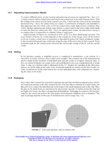
chips. A chip on a finished wafer is illustrated in Fig. 1.7. Despite the caretaken in the fabrication
process, not all the chips on the wafer work. Automated methods are used to test the microscopic cir-
cuitry of each device on the wafer before it is cut into individual chips with a diamond saw, separat-
ing the chips on the wafer.
1.6.9 Packaging
Each chip is then inserted into a protective package that provides mechanical support and an electri-
cal connection interface with other external devices. The tiny chip is mounted on a metal frame, and
thin gold wires connect the individual pin on the frame to the small aluminum pad on the chip. Thus,
the pins on the metal frame are attached to the microscopic circuitry. To further protect the chip and
its fragile wire bonds, the chip is encapsulated in hard plastic. Packaging also removes the heat gen-
3
erated by the circuit and protects the chip against environmental conditions such as humidity. The
type of package depends on the type of microprocessor and its usage (Fig. 1.8).
FIGURE 1.7 Each square represents a chip on a finished wafer.
Downloaded from Digital Engineering Library @ McGraw-Hill (www.digitalengineeringlibrary.com)
Copyright © 2004 The McGraw-Hill Companies. All rights reserved.
Any use is subject to the Terms of Use as given at the website.