Page 16 - Semiconductor Manufacturing Handbook
P. 16

Geng(SMH)_CH02.qxd  04/04/2005  19:33  Page 2.3


                                                            IC DESIGN

                                                                                              IC DESIGN  2.3


                                                        Collector                       Collector
                                                       p                              n

                                              Base                            Base
                                                       n                              p

                                                       p                               n

                                                         Emitter                        Emitter


                                                            C                              C

                                                 B                               B


                                                            E                              E
                                              FIGURE 2.2  BJTs—npn and pnp—symbolic representation.


                                    Another type of transistor, and one that is used in a majority of digital integrated circuits today,
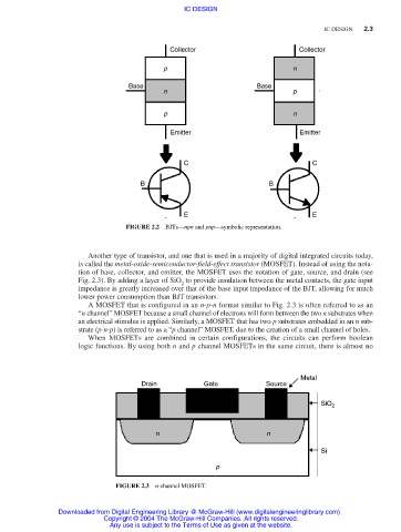
                                  is called the metal-oxide-semiconductor-field-effect transistor (MOSFET). Instead of using the nota-
                                  tion of base, collector, and emitter, the MOSFET uses the notation of gate, source, and drain (see
                                  Fig. 2.3). By adding a layer of SiO to provide insulation between the metal contacts, the gate input
                                                           2
                                  impedance is greatly increased over that of the base input impedance of the BJT, allowing for much
                                  lower power consumption than BJT transistors.
                                    A MOSFET that is configured in an n-p-n format similar to Fig. 2.3 is often referred to as an
                                  “n channel” MOSFET because a small channel of electrons will form between the two n substrates when
                                  an electrical stimulus is applied. Similarly, a MOSFET that has two p substrates embedded in an n sub-
                                  strate (p-n-p) is referred to as a “p channel” MOSFET, due to the creation of a small channel of holes.
                                    When MOSFETs are combined in certain configurations, the circuits can perform boolean
                                  logic functions. By using both n and p channel MOSFETs in the same circuit, there is almost no


                                                                                        Metal
                                                 Drain           Gate           Source

                                                                                             SiO 2


                                                     n                          n

                                                                                             Si
                                                                    p

                                           FIGURE 2.3  n-channel MOSFET.


                             Downloaded from Digital Engineering Library @ McGraw-Hill (www.digitalengineeringlibrary.com)
                                        Copyright © 2004 The McGraw-Hill Companies. All rights reserved.
                                          Any use is subject to the Terms of Use as given at the website.
   11   12   13   14   15   16   17   18   19   20   21