
Page 18 - Semiconductor Manufacturing Handbook
P. 18
Geng(SMH)_CH02.qxd 04/04/2005 19:33 Page 2.5
IC DESIGN
IC DESIGN 2.5
2.5 DESIGNING AN IC
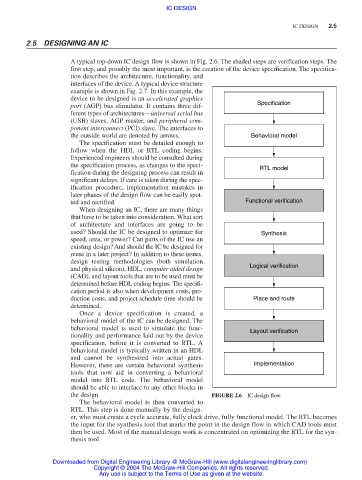
A typical top-down IC design flow is shown in Fig. 2.6. The shaded steps are verification steps. The
first step, and possibly the most important, is the creation of the device specification. The specifica-
tion describes the architecture, functionality, and
interfaces of the device. A typical device structure
example is shown in Fig. 2.7. In this example, the
device to be designed is an accelerated graphics
Specification
port (AGP) bus stimulator. It contains three dif-
ferent types of architectures—universal serial bus
(USB) slaves, AGP master, and peripheral com-
ponent interconnect (PCI) slave. The interfaces to
the outside world are denoted by arrows. Behavioral model
The specification must be detailed enough to
follow when the HDL or RTL coding begins.
Experienced engineers should be consulted during
the specification process, as changes to the speci-
RTL model
fication during the designing process can result in
significant delays. If care is taken during the spec-
ification procedure, implementation mistakes in
later phases of the design flow can be easily spot-
ted and rectified. Functional verification
When designing an IC, there are many things
that have to be taken into consideration. What sort
of architecture and interfaces are going to be
used? Should the IC be designed to optimize for Synthesis
speed, area, or power? Can parts of the IC use an
existing design? And should the IC be designed for
reuse in a later project? In addition to these issues,
design testing methodologies (both simulation
and physical silicon), HDL, computer aided design Logical verification
(CAD), and layout tools that are to be used must be
determined before HDL coding begins. The specifi-
cation period is also when development costs, pro-
duction costs, and project schedule time should be Place and route
determined.
Once a device specification is created, a
behavioral model of the IC can be designed. The
behavioral model is used to simulate the func- Layout verification
tionality and performance laid out by the device
specification, before it is converted to RTL. A
behavioral model is typically written in an HDL
and cannot be synthesized into actual gates.
However, there are certain behavioral synthesis Implementation
tools that now aid in converting a behavioral
model into RTL code. The behavioral model
should be able to interface to any other blocks in
the design. FIGURE 2.6 IC design flow.
The behavioral model is then converted to
RTL. This step is done manually by the design-
er, who must create a cycle accurate, fully clock drive, fully functional model. The RTL becomes
the input for the synthesis tool that marks the point in the design flow in which CAD tools must
then be used. Most of the manual design work is concentrated on optimizing the RTL for the syn-
thesis tool.
Downloaded from Digital Engineering Library @ McGraw-Hill (www.digitalengineeringlibrary.com)
Copyright © 2004 The McGraw-Hill Companies. All rights reserved.
Any use is subject to the Terms of Use as given at the website.