
Page 23 - Semiconductor Manufacturing Handbook
P. 23
Geng(SMH)_CH03.qxd 04/04/2005 19:34 Page 3.2
SILICON SUBSTRATES FOR SEMICONDUCTOR MANUFACTURING
3.2 SEMICONDUCTOR FUNDAMENTALS AND BASIC MATERIALS
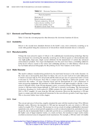
TABLE 3.1 Electronic Function of Silicon
Physical properties
Band gap, eV 1.45
Relative dielectricconstant 11.7
Thermal conductivity, W/cm-K 1.45
Lattice electron mobility, V/cm 2 1350
Lattice hole mobility, V/cm 2 480
Breakdown electric field, V/cm 3 X 5e 10
3.2.1 Electronic and Thermal Properties
Table 3.1 lists the relevant properties that determine the electronic function of silicon.
3.2.2 Availability
Silicon is the second most abundant element in the Earth’s crust, most commonly occurring as its
oxide with quartzite being the common ore of silicon from which elemental silicon is extracted.
3.2.3 Manufacturability
Perhaps the most attractive aspect of silicon is the sophisticated manufacturing technology that has
been developed for converting the naturally occurring ore of silicon (quartz or silicon dioxide) into
very high-quality, large-area, single crystal substrates for the manufacture of current day advanced
semiconductor products. Two major developments over the years have been a continuing reduction
in the levels of heavy metals in the wafers and continuing advances in wafer flatness which in turn
has facilitated advanced lithography for the printing of ever finer features on the wafers.
3.2.4 Wafer Diameter
The need to enhance manufacturing productivity has motivated increases in the wafer diameter. As
the wafer area is increased by more than two times, the cost of a new tool set for wafer fabrication
is found to increase only by 30 to 40 percent and the total cost per area of a processed wafer is found
to decrease by 30 to 50 percent. Since this is a major activity that has to address the growth—and
conversion into wafers—of larger diameter ingots and the development of a full complement of
wafer processing equipment, the transition in wafer diameters took approximately a decade. A tran-
sition to 200 mm wafers, from 150 mm diameter wafers, occurred at around 1990 and the initial con-
version to 300 mm wafers began haltingly in 1999 and is currently accelerating. The International
Technology Roadmap for Semiconductors (ITRS) projects the next transition to 450 mm in about
1
2011 to 2012, roughly 10 years from the 300-mm conversion. However, the transition to 450 mm
ingots is a major step with new physical limitations for the cost-effective growth of such large ingots.
This is discussed further later in this chapter.
3.2.5 Cost
The cost per unit area of silicon has, roughly, remained the same with the transition from 150 to 200 mm
diameter wafers. However, the transition to 300 mm has increased the unit cost relative to 200 mm
wafers by roughly 50 to 75 percent. This increase in cost as a result of scaling is attributable to increased
equipment costs, such as crystal growth equipment, as well as reduced productivity, particularly in crys-
tal growth, due to fundamental limits to achievable growth rate as crystal diameter is increased. Despite
the higher costs of larger diameter wafers, on a total cost basis, the transition to larger wafers makes
excellent economical sense in integrated circuit manufacture. For example, a 300-mm wafer will enable
Downloaded from Digital Engineering Library @ McGraw-Hill (www.digitalengineeringlibrary.com)
Copyright © 2004 The McGraw-Hill Companies. All rights reserved.
Any use is subject to the Terms of Use as given at the website.