
Page 27 - Semiconductor Manufacturing Handbook
P. 27
Geng(SMH)_CH03.qxd 04/04/2005 19:34 Page 3.6
SILICON SUBSTRATES FOR SEMICONDUCTOR MANUFACTURING
3.6 SEMICONDUCTOR FUNDAMENTALS AND BASIC MATERIALS
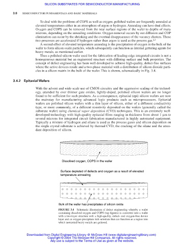
To deal with the problems of COPS as well as oxygen, polished wafers are frequently annealed at
elevated temperatures either in an atmosphere of argon or hydrogen. Annealing can have dual effects.
Oxygen and COPS can be removed from the near surface regions of the wafer to depths of many
microns, depending on the annealing conditions. Oxygen removal occurs by out diffusion and COP
elimination can occur by the shrinking and the eventual disappearance of the vacancy clusters. These
two processes are accelerated if hydrogen rather than argon is used as the process gas. 2,3
A second effect of elevated temperature annealing is the precipitation of oxygen in the bulk of the
wafer to form silicon oxide particles, which subsequently can function as internal gettering agents for
heavy metals, as mentioned earlier.
Thus a polished silicon wafer used for the fabrication of leading-edge integrated circuits is not a
homogeneous material but an engineered structure with differing surface and bulk properties. The
concept of defect engineering has been well developed to achieve high-quality, defect-free surfaces
where the active devices reside and a two-phase material with a distribution of silicon dioxide parti-
cles in a silicon matrix in the bulk of the wafer. This is shown, schematically in Fig. 3.4.
3.4.2 Epitaxial Wafers
With the advent and wide-scale use of CMOS circuitry and the aggressive scaling of the technol-
ogy, attended by ever thinner gate oxides, lightly-doped, polished silicon wafers are no longer
found to be sufficient for such products. As a consequence, epitaxial (epi) silicon wafers are now
the mainstay for manufacturing advanced logic products such as microprocessors. Epitaxial
wafers are polished silicon wafers with a thin layer of silicon, either of a different conductivity
type, or more commonly, of a different resistivity deposited on the wafers (generally called the
substrate wafer) using chemical vapor deposition (CVD) techniques. This is an extremely well-
developed technology with high-quality epitaxial films ranging in thickness from about 1 µm to
several microns for integrated circuit fabrication manufactured in highly automated equipment.
Typically a mixture of hydrogen and silane is used as the process gases and silicon deposition on
the single crystal substrate is achieved by thermal CVD, the cracking of the silane and the atten-
dant deposition of silicon.
Dissolved oxygen, COPS in the wafer
Surface depleted of defects and oxygen as a result of elevated
temperature annealing
Bulk of the wafer has precipitates of silicon oxide
FIGURE 3.4 Schematic illustration of defect engineering whereby a wafer
containing dissolved oxygen and COPS (top figures) is converted into a wafer
with a two-layer structure with a high-quality, defect- and oxygen-free device
layer and an oxygen precipitate rich substrate that can function as a region into
which unwanted heavy metals are gettered.
Downloaded from Digital Engineering Library @ McGraw-Hill (www.digitalengineeringlibrary.com)
Copyright © 2004 The McGraw-Hill Companies. All rights reserved.
Any use is subject to the Terms of Use as given at the website.