
Page 30 - Semiconductor Manufacturing Handbook
P. 30
Geng(SMH)_CH03.qxd 04/04/2005 19:34 Page 3.9
SILICON SUBSTRATES FOR SEMICONDUCTOR MANUFACTURING
SILICON SUBSTRATES FOR SEMICONDUCTOR MANUFACTURING 3.9
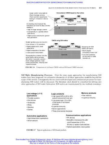
Larger junction area leads to: Conventional CMOS based on Epi wafers
-Higher leakage currents
-Higher junction capacitance N+ P+
leading to limitations in device
N+ N+ STI P+ P+
speed
P-well N-well
Conducting silicon beneath the Epitaxial layer
transistors can result in stray currents
leading to:
• High off-stage leakage currents
Substrate
• Susceptibility to a-particle effects
(soft errors)
• Higher power consumption, greater
heat generation
CMOS using SOI wafers
Smaller junction area can result in:
• Low voltage (<1 V) operation N+ P+
• Higher speed due to lower Designing with SOI
N+ N+ P+ P+
capacitance wafers can lead to:
Buried oxide
• Higher temperature operation • Much simpler
• Lower power consumption processing—lower cost
Substrate • Low cost substrates
Decoupling the substrate from the
can be used for wafer
active silicon volume enables manufacture
elimination of parasitic currents—
lower voltage operation, lower
power consumption, immunity from
a-particle events
FIGURE 3.6 Comparison of epi-based CMOS with an SOI-based CMOS structure.
SOI Wafer Manufacturing Processes. Over the years many approaches for manufacturing SOI
wafers have been proposed. An exhaustive discussion of all these approaches would be beyond the
scope of this review. Consequently the two most well-developed and commercial processes for man-
ufacturing SOI wafers will be discussed. The literature cited should be consulted for delving into
other approaches of SOI wafer fabrication. SOI wafers are manufactured by two methods nowadays:
Low-voltage (<1 V) Logic products Memory products
applications • High-speed MPUs (20 to 30% • Fast memory
• Portable systems speed improvement over epi) • A particle immunity
• Cell phones • Low-power logic (15 to 50%
• Notebooks of the levels of epi-based
products)
• PDAs
• A particle immunity
• Watches
• Server applications
• Games
• Three-dimensional structures
Automotive applications Communications applications
• RF devices
• High-temperature applications
• Monolithic microwave ICs with
• Smart sensors
cutoff frequencies of 20 to
30 GHz to replace GaAs devices
• Optical applications–wave guides
FIGURE 3.7 Typical applications of SOI-based products.
Downloaded from Digital Engineering Library @ McGraw-Hill (www.digitalengineeringlibrary.com)
Copyright © 2004 The McGraw-Hill Companies. All rights reserved.
Any use is subject to the Terms of Use as given at the website.