
Page 33 - Semiconductor Manufacturing Handbook
P. 33
Geng(SMH)_CH03.qxd 04/04/2005 19:34 Page 3.12
SILICON SUBSTRATES FOR SEMICONDUCTOR MANUFACTURING
3.12 SEMICONDUCTOR FUNDAMENTALS AND BASIC MATERIALS
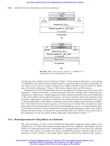
n+ Poly
SiO 2
n+ Strained Si n+
source drain
Relaxed Si 0.7 Ge 0.3
Relaxed graded Si 1−y Ge layer
y
Y = 0 to 0.3
Si substrate
(a)
n+ Poly
SiO 2
n+ Strained Si n+
source drain
Relaxed Si 0.7 Ge 0.3
Ge layer
Relaxed graded Si 1−y y
Y = 0 to 0.3
Buried SiO 2
Si substrate
(b)
FIGURE 3.10 Cross-sectional structures of MOSFETs in
strained silicon and in strained silicon on oxide.
reported for a Ge content of about 20 percent. Figure. 3.10(a) schematically shows a cross section
of a MOSFET with strained silicon channel based on using Si-Ge alloys to induce strain in the sili-
con. There is also a drive to combine strained silicon wafers with SOI wafers to achieve the advan-
12
tages of both the technologies. Figure 3.10(b) shows strained silicon on SOI structure.
Although the use of Si-Ge intermediate layers is one approach to introducing strain in silicon, this
represents a wafer-level solution to strain introduction with the incoming wafer already having a
strained layer on the surface. Another approach to strain introduction involves the local modification
of the silicon surface during wafer processing to selectively introduce strain in the channels of the
transistors. Approaches for doing this include the use of thermal-expansion-mismatched films, such
as silicon nitride films, on the surface to introduce strain in the channel of the transistors, modifica-
tion of the shallow trench isolation process as well as the use of silicide films on transistor source/
drain regions for strain introduction. This local strain introduction process, as distinct from the glob-
al Si-Ge based approach to strain introduction, has many potential advantages such as more control,
during wafer processing, over the process and potentially lower costs. Based on the current state of
the technology it is not clear which of these approaches will dominate in future. 13,14,15
3.4.5 Novel Approaches for Using Silicon as a Substrate
The major advantage of silicon is the availability of high-quality, large-area silicon wafers at rea-
sonable prices. No other semiconductor material approaches the availability, affordability, and fea-
sibility for scaling that silicon does. Consequently an emerging trend is to use silicon as a substrate
for other, more-expensive or smaller-area wafers with differing electronic properties. This is not, as
discussed in earlier sections, a new trend. Silicon epitaxy, with the top epitaxial layer having a
Downloaded from Digital Engineering Library @ McGraw-Hill (www.digitalengineeringlibrary.com)
Copyright © 2004 The McGraw-Hill Companies. All rights reserved.
Any use is subject to the Terms of Use as given at the website.