
Page 35 - Semiconductor Manufacturing Handbook
P. 35
Geng(SMH)_CH03.qxd 04/04/2005 19:34 Page 3.14
SILICON SUBSTRATES FOR SEMICONDUCTOR MANUFACTURING
3.14 SEMICONDUCTOR FUNDAMENTALS AND BASIC MATERIALS
2. The drive toward larger wafer sizes as contemplated by the ITRS.
3. The combining of nonsilicon materials with silicon—SOI wafers being at the forefront of this
trend and other technologies/materials such as strained silicon, germanium, and compound semi-
conductors on silicon—is forming topics of world-wide research.
A brief discussion of silicon wafer quality and scaling issues are discussed in the following sections.
3.5.1 Wafer Quality
Tremendous progress has been made over the last decade and half in reducing the size and density
of particles on silicon wafers. Particles, which are generally foreign material of organic or inorganic
origin or due to COPS in the ingots, have tracked with the technology generations. According to
the ITRS, the particle size on the wafers is taken to be equal to the technology generation, i.e., the
critical dimension of the transistor. For example, the particle size specification on wafers used for
leading-edge products today (2004) would be 90 nm since current leading-edge products are man-
ufactured using 90-nm technology. These sizes are expected to be dramatically reduced to keep up
with the ITRS.
Another wafer parameter of critical importance is wafer flatness. The one that has been empha-
sized over the years is site flatness. This is the flatness within a specified site, which is the area over
which lithography is conducted in a step and repeat lithography tool, on the wafer. Typically a site
size of 25 mm by 25 mm is prescribed with a 32-mm by 8-mm site size being specified when more
contemporary scanning steppers are used. Site flatness variations on the wafer surface can lead to
focus failures in lithography. This parameter addresses surface-height variations of the order of the
depth of focus of the lithography tool over spatial wavelengths of tens of mm. A separate and more
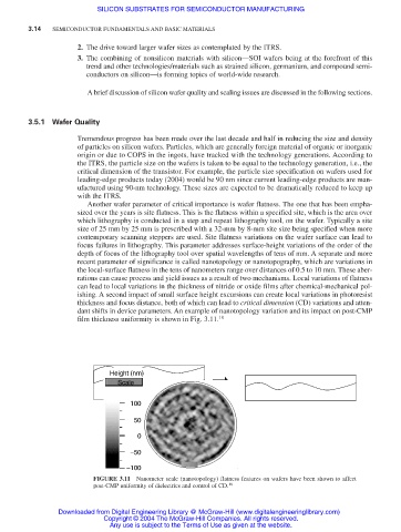
recent parameter of significance is called nanotopology or nanotopography, which are variations in
the local-surface flatness in the tens of nanometers range over distances of 0.5 to 10 mm. These aber-
rations can cause process and yield issues as a result of two mechanisms. Local variations of flatness
can lead to local variations in the thickness of nitride or oxide films after chemical-mechanical pol-
ishing. A second impact of small surface height excursions can create local variations in photoresist
thickness and focus distance, both of which can lead to critical dimension (CD) variations and atten-
dant shifts in device parameters. An example of nanotopology variation and its impact on post-CMP
film thickness uniformity is shown in Fig. 3.11. 18
Height (nm)
Scale
100
50
0
−50
−100
FIGURE 3.11 Nanometer scale (nanotopology) flatness features on wafers have been shown to affect
post-CMP uniformity of dielectrics and control of CD. 18
Downloaded from Digital Engineering Library @ McGraw-Hill (www.digitalengineeringlibrary.com)
Copyright © 2004 The McGraw-Hill Companies. All rights reserved.
Any use is subject to the Terms of Use as given at the website.