
Page 39 - Semiconductor Manufacturing Handbook
P. 39
Geng(SMH)_CH04.qxd 04/04/2005 19:36 Page 4.2
COPPER, LOW-k DIELECTRICS, AND THEIR RELIABILITY
4.2 SEMICONDUCTOR FUNDAMENTALS AND BASIC MATERIALS
2.5
2.0 Interconnect delay (RC)
Delay time (×10 −9 sec) 1.5
1.0
Intrinsic gate delay
0.5
0
0 0.5 1.0 1.5 2.0 2.5 3.0 3.5
Feature size (µm)
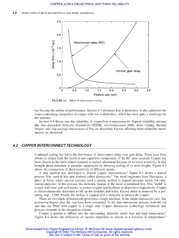
FIGURE 4.1 Effect of interconnect scaling.
has become the metric of performance. Section 4.3 discusses low-κ dielectrics. It also addresses the
issues concerning integration of copper with low-k dielectrics, which has been quite a challenge for
the industry.
Section 4.4 delves into the reliability of copper/low-k interconnects. Typical reliability stresses
like time-dependent dielectric breakdown (TDDB), electromigration (EM), stress voiding, thermal
fatigue, and chip package interactions (CPIs) are described. Factors affecting these reliability mech-
anisms are discussed.
4.2 COPPER INTERCONNECT TECHNOLOGY
Continual scaling has led to the dominance of interconnect delay over gate delay. There have been
efforts to reduce both the resistive and capacitive components of the RC time constant. Copper has
been chosen as the interconnect material to replace aluminum because of its lower resistivity. It also
brought about reduction in parasitic capacitance by allowing scaling of 1x level heights. Figure 4.2
shows the comparison of sheet resistivity of different metals.
3
A new method was developed to deposit copper interconnects. Figure 4.3 shows a typical
2
process flow used in this new method called damascene. The word originates from Damascus, a
place in Syria, where ancient jewelers used a similar method to deposit precious metals for orna-
mental purposes. In this process, the dielectric instead of the metal is patterned first. This “mold” is
coated with liner and seed layers, to protect copper and facilitate its deposition respectively. Copper
is electrochemically deposited to fill up the trenches and holes. Excess metal is removed by a pol-
ishing step—CMP. Finally the surface is capped with a dielectric to protect the copper.
There are two kinds of damascene processes—single and dual. In the single-damascene case, line
processing begins after the vias have been completed. In the dual-damascene process, both the via
and line are filled with copper in a single step. Copper damascene technology introduced new
process elements in the integration scheme.
Copper is known to diffuse into the surrounding dielectric under bias and high temperature. 5
Figure 4.4 shows the diffusivity of various impurities in silicon as a function of temperature. 6
Downloaded from Digital Engineering Library @ McGraw-Hill (www.digitalengineeringlibrary.com)
Copyright © 2004 The McGraw-Hill Companies. All rights reserved.
Any use is subject to the Terms of Use as given at the website.